Publications
ResearcherID : C-5956-2008 (TY, h-index: 25) , AAZ-8749-2021 (RK, h-index: 13)
Google Scholar : TY (h-index: 35), RK (h-index: 14), KT (h-index: 4)
Research Square: TY
2025
Kosuke Takada, Ryota Katsumi, Daichi Sato, Kenta Kawai, Takashi Yatsui
High-Q plasmonic resonances from a transfer-printed diamond ring on a silver surface Journal Article
In: Japanese Journal of Applied Physics, vol. 64, iss. 8, pp. 080903, 2025.
Abstract | Links | BibTeX | タグ: Diamond, nanophotonics, Plasmon
@article{plasmonicring,

title = {High-Q plasmonic resonances from a transfer-printed diamond ring on a silver surface},

author = {Kosuke Takada and Ryota Katsumi and Daichi Sato and Kenta Kawai and Takashi Yatsui},

doi = {10.35848/1347-4065/adf618},

year  = {2025},

date = {2025-08-14},

journal = {Japanese Journal of Applied Physics},

volume = {64},

issue = {8},

pages = {080903},

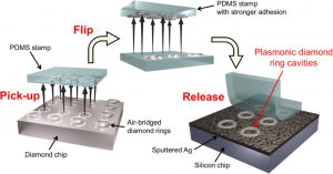
abstract = {Optically addressable point defects in diamond are promising physical platforms in quantum technologies. In particular, defects embedded in plasmonic devices can interact strongly with photons and provide a robust approach to engineering spin-photon interfaces. However, diamond-based plasmonic devices have low quality factors of Q<10, constrained by fabrication difficulties. This study demonstrates the high-Q plasmonic resonance of optical emissions from nitrogen-vacancy centers in diamond ring structures onto a silver surface, and experimentally shows that Q~179. The proposed device can be easily fabricated using the transfer printing technique. These results address the lack of high-Q plasmonic cavities in diamond-based technologies.},

keywords = {Diamond, nanophotonics, Plasmon},

pubstate = {published},

tppubtype = {article}

}
Kosuke Takada, Ryota Katsumi, Kenta Kawai, Daichi Sato, Takashi Yatsui
Alignment-tolerant hybrid integration of a diamond quantum sensor on a silicon nitride photonic waveguide Journal Article
In: Optics Express, vol. 33, iss. 11, pp. 22769-22779, 2025.
Abstract | Links | BibTeX | タグ: Diamond, nanophotonics
@article{alignmentfree,

title = {Alignment-tolerant hybrid integration of a diamond quantum sensor on a silicon nitride photonic waveguide},

author = {Kosuke Takada and Ryota Katsumi and Kenta Kawai and Daichi Sato and Takashi Yatsui},

doi = {10.1364/OE.559486},

year  = {2025},

date = {2025-05-24},

urldate = {2025-05-24},

journal = {Optics Express},

volume = {33},

issue = {11},

pages = {22769-22779},

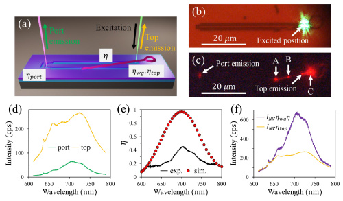
abstract = {Hybrid-integrated photonic circuits play a crucial role in recent quantum technologies. However, deterministic and alignment-tolerant methods are still lacking, and their development is crucial for accelerating the scalable fabrication of quantum systems. In this study, we demonstrate alignment-tolerant coupling between diamond and silicon nitride waveguides using the deterministic transfer-printing method. To validate this approach, we also demonstrate the capability of on-chip quantum sensing using nitrogen vacancy centers in diamond waveguides. These results pave the way for compact packaging of highly sensitive quantum sensors based on photonic integrated circuits.},

keywords = {Diamond, nanophotonics},

pubstate = {published},

tppubtype = {article}

}
Ryota Katsumi, Kosuke Takada, Fedor Jelezko, Takashi Yatsui
Recent progress in hybrid diamond photonics for quantum information processing and sensing Journal Article
In: Communications Engineering, vol. 4, pp. 85, 2025.
Abstract | Links | BibTeX | タグ: Diamond, Review
@article{review2025,

title = {Recent progress in hybrid diamond photonics for quantum information processing and sensing},

author = {Ryota Katsumi and Kosuke Takada and Fedor Jelezko and Takashi Yatsui},

doi = {10.1038/s44172-025-00398-2},

year  = {2025},

date = {2025-05-08},

journal = {Communications Engineering},

volume = {4},

pages = {85},

abstract = {Point defects in diamond, particularly nitrogen-vacancy (NV) centers, have emerged as powerful tools for a broad range of quantum technologies. These defects are promising candidates for quantum information science, serving as deterministic single-photon sources and solid-state quantum memories. They have also been employed as nanoscale quantum sensors to detect various physical quantities, including magnetic fields, electric fields, and temperature, owing to their long spin coherence time at room temperature. Development of these diamond-based quantum technologies has been rapidly boosted by a recent quantum leap in nanofabrication technologies for high-quality single-crystal diamond. Incorporating these color centers into diamond nanostructures with mature integrated photonics provides a promising route to build scalable and practical systems for quantum applications. This review discusses recent progress and challenges in the hybrid integration of diamond color centers on cutting-edge photonic platforms.},

keywords = {Diamond, Review},

pubstate = {published},

tppubtype = {article}

}
Ryota Katsumi, Kosuke Takada, Kenta Kawai, Daichi Sato, Takashi Yatsui
High-sensitivity nanoscale quantum sensors based on a diamond micro-resonator Journal Article
In: Communications Materials, vol. 6, pp. 49, 2025.
Abstract | Links | BibTeX | タグ: Diamond
@article{ring2025,

title = {High-sensitivity nanoscale quantum sensors based on a diamond micro-resonator},

author = {Ryota Katsumi and Kosuke Takada and Kenta Kawai and Daichi Sato and Takashi Yatsui},

doi = {10.1038/s43246-025-00770-x},

year  = {2025},

date = {2025-03-18},

urldate = {2025-03-18},

journal = {Communications Materials},

volume = {6},

pages = {49},

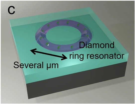
abstract = {Nitrogen-vacancy centers have demonstrated significant potential as quantum magnetometers for nanoscale phenomena and sensitive field detection, attributed to their exceptional spin coherence at room temperature. However, it is challenging to achieve solid-state magnetometers that can simultaneously possess high spatial resolution and high field sensitivity. Here we demonstrate nanoscale quantum sensing with high field sensitivity by using on-chip diamond micro-ring resonators. The ring resonator enables the efficient use of photons by confining them in a nanoscale region, enabling the magnetic sensitivity of 1.0 μT/sqrt{{mbox{Hz}}} on a photonic chip with a measurement contrast of theoretical limit. We also show that the proposed on-chip approach can improve the sensitivity via efficient light extraction with photonic waveguide coupling. Our work provides a pathway toward the development of chip-scale packaged sensing devices that can detect various nanoscale physical quantities for fundamental science, chemistry, and medical applications.},

keywords = {Diamond},

pubstate = {published},

tppubtype = {article}

}
2024
Kosuke Takada, Ryota Katsumi, Takashi Yatsui
Sensitivity improvement of a single-NV diamond magnetometer using a chiral waveguide Journal Article
In: Optics Express, vol. 32, iss. 1, pp. 795-802, 2024.
Abstract | Links | BibTeX | タグ: Diamond
@article{takada_chiral,

title = {Sensitivity improvement of a single-NV diamond magnetometer using a chiral waveguide},

author = {Kosuke Takada and Ryota Katsumi and Takashi Yatsui},

doi = {10.1364/OE.509860},

year  = {2024},

date = {2024-01-01},

urldate = {2024-01-01},

journal = {Optics Express},

volume = {32},

issue = {1},

pages = {795-802},

abstract = {A single nitrogen-vacancy (NV) center in diamond is utilized to perform nanoscale magnetic measurements. However, the low contrast and poor collection efficiency of spin-dependent emitted photons limited the instrument sensitivity to approximately several nT/√Hz. Here, we design a diamond magnetometer based on a chiral waveguide. We numerically demonstrate that the proposed device achieves a sensitivity of 170 pT/√Hz owing to near-unity contrast and efficient photon collection. We also confirm that the device sensitivity is robust against position misalignment and dipole misorientation of an NV center. The proposed approach will enable the construction of a highly-sensitive magnetometer with high spatial resolution.},

keywords = {Diamond},

pubstate = {published},

tppubtype = {article}

}
2023
Ryota Katsumi, Kosuke Takada, Shun Naruse, Kenta Kawai, Daichi Sato, Takeshi Hizawa, Takashi Yatsui
Hybrid integration of ensemble nitrogen-vacancy centers in single-crystal diamond based on pick-flip-and-place transfer printing Journal Article
In: Applied Physics Letters, vol. 123, iss. 11, pp. 111108, 2023.
Abstract | Links | BibTeX | タグ: Diamond, NV center
@article{katsumi23flip,

title = {Hybrid integration of ensemble nitrogen-vacancy centers in single-crystal diamond based on pick-flip-and-place transfer printing },

author = {Ryota Katsumi and Kosuke Takada and Shun Naruse and Kenta Kawai and Daichi Sato and Takeshi Hizawa and Takashi Yatsui},

doi = {10.1063/5.0161268},

year  = {2023},

date = {2023-09-13},

urldate = {2023-09-13},

journal = {Applied Physics Letters},

volume = {123},

issue = {11},

pages = {111108},

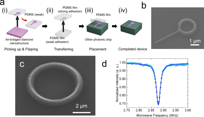
abstract = {Incorporating color centers in diamond with mature integrated photonics using hybrid integration techniques such as transfer printing provides a promising route toward scalable quantum applications. However, single-crystal diamond nanostructures fabricated using current etching technologies have triangular bottoms that are unsuitable for conventional pick-and-place integration. Herein, we present an alternative approach for deterministically integrating diamond nanostructures on chip. We demonstrate the hybrid integration of a diamond triangular nanobeam containing a nitrogen-vacancy ensemble on an SiO2 chip by picking it up using a weak adhesive film, flipping it, and transferring it to a stronger one. This “pick-flip-and-place” approach provides a flat diamond-chip interface, enabling the high-yield hybrid integration regardless of the shape of diamond nanostructures. Additionally, diamond nanofabrication is facilitated by transfer-printing hard masks for diamond etching. We also show that the integrated diamond nanobeam functions as a nanoscale quantum sensor. Our proposed approach paves the way toward scalable hybrid-diamond quantum photonics.},

keywords = {Diamond, NV center},

pubstate = {published},

tppubtype = {article}

}
Kenji Iida, Takashi Takeuchi, Ryota Katsumi, Takashi Yatsui
Variations in the Photoexcitation Mechanism of an Adsorbed Molecule on a Gold Nanocluster Governed by Interfacial Contact Journal Article
In: The Journal of Physical Chemistry A, vol. 127, iss. 37, pp. 7718-7726, 2023.
Abstract | Links | BibTeX | タグ: photoexcitation
@article{iida23,

title = {Variations in the Photoexcitation Mechanism of an Adsorbed Molecule on a Gold Nanocluster Governed by Interfacial Contact},

author = {Kenji Iida and Takashi Takeuchi and Ryota Katsumi and Takashi Yatsui},

doi = {10.1021/acs.jpca.3c03775},

year  = {2023},

date = {2023-09-08},

urldate = {2023-09-08},

journal = {The Journal of Physical Chemistry A},

volume = {127},

issue = {37},

pages = {7718-7726},

abstract = {We performed first-principles calculations on the optical response of a Au147–azobenzene complex to elucidate the role of the interfacial contact between Au147 and azobenzene. Our calculations of photoexcited electron dynamics for different configurations of azobenzene adsorbed on the Au147 nanocluster revealed that the optical properties of the azobenzene moiety change markedly by the interfacial contact, even if the electronic structure in the ground state is almost unchanged. The optical absorption measured for isolated azobenzene weakens when the Au147–azobenzene interaction increases, while the absorption measured using the light field along the Au147–azobenzene alignment strengthens. The electronic excitation analysis showed that the mechanism of the charge-transfer excitation between Au147 and azobenzene changes remarkably depending on the strength of the interfacial interaction. We revealed that the optical property can be governed by the atomic-scale difference in the adsorption structure of azobenzene on a Au147 nanocluster. This study affords novel insights that could enable the photoexcitation mechanism to be controlled by designing the interface between a metal nanoparticle and a molecule.},

keywords = {photoexcitation},

pubstate = {published},

tppubtype = {article}

}
Ryuichi Hirota, Toru Murayama, Ryota Katsumi, Tokuhisa Kawawaki, Shin Yabukami, Ryuji Igarashi, Yuichi Negishi, Moriaki Kusakabe, Masaki Sekino, Takashi Yatsui, Akihiro Kuwahata
Rapid virus detection using magnetic second harmonics of superparamagnetic iron oxide nanoparticles Journal Article
In: AIP Advances, vol. 13, pp. 025144, 2023.
Abstract | Links | BibTeX | タグ: Virus Detection
@article{virusNPs,

title = {Rapid virus detection using magnetic second harmonics of superparamagnetic iron oxide nanoparticles},

author = {Ryuichi Hirota and Toru Murayama and Ryota Katsumi and Tokuhisa Kawawaki and Shin Yabukami and Ryuji Igarashi and Yuichi Negishi and Moriaki Kusakabe and Masaki Sekino and Takashi Yatsui and Akihiro Kuwahata},

doi = {10.1063/9.0000483},

year  = {2023},

date = {2023-02-09},

urldate = {2023-02-09},

journal = {AIP Advances},

volume = {13},

pages = {025144},

abstract = {Virus detection methods based on nonlinear magnetic response of magnetic nanoparticles have been investigated, and magnetic detection methods using the third harmonic are widely applied, owing to their high sensitivity and short measurement time. This paper proposes a virus detection method based on the second harmonic because of its larger signal component. We found that the second harmonic signal is superior to the third harmonic signal for small nanobeads and a large change of the second harmonic signal in the signal-to-noise ratio (SNR) with nanobeads concentration. In addition, a virus detection limit of 100 pg/ml is achieved. Therefore, the proposed method can potentially be utilized for rapid screening of viruses.},

keywords = {Virus Detection},

pubstate = {published},

tppubtype = {article}

}
2022
Ryota Katsumi, Takeshi Hizawa, Akihiro Kuwahata, Shun Naruse, Yuji Hatano, Takayuki Iwasaki, Mutsuko Hatano, Fedor Jelezko, Shinobu Onoda, Takeshi Ohshima, Masaki Sekino, Takashi Yatsui
Transfer-printing-based integration of silicon nitride grating structure on single-crystal diamond toward sensitive magnetometers Journal Article
In: Applied Physics Letters, vol. 121, iss. 16, pp. 161103, 2022.
Abstract | Links | BibTeX | タグ: Diamond, magnetometer
@article{katsumi_grating,

title = {Transfer-printing-based integration of silicon nitride grating structure on single-crystal diamond toward sensitive magnetometers},

author = {Ryota Katsumi and Takeshi Hizawa and Akihiro Kuwahata and Shun Naruse and Yuji Hatano and Takayuki Iwasaki and Mutsuko Hatano and Fedor Jelezko and Shinobu Onoda and Takeshi Ohshima and Masaki Sekino and Takashi Yatsui},

doi = {10.1063/5.0107854},

year  = {2022},

date = {2022-10-19},

urldate = {2022-10-19},

journal = {Applied Physics Letters},

volume = {121},

issue = {16},

pages = {161103},

abstract = {Negatively charged nitrogen-vacancy (NV) centers in diamond have emerged as promising candidates for a wide range of quantum applications, especially quantum sensing of magnetic field. Implementation of nanostructure into diamond is powerful for efficient photon collection of NV centers and chip-scale miniaturization of the device, which is crucial for sensitive and practical diamond magnetometers. However, fabrication of the diamond nanostructure involves technical limitations and can degrade the spin coherence of the NV centers. In this study, we demonstrate the hybrid integration of a silicon nitride grating structure on a single-crystal diamond by utilizing transfer printing. This approach allows the implementation of the nanostructure in diamond using a simple pick-and-place assembly, facilitating diamond-based quantum applications without any complicated diamond nanofabrication. We observed the intensity enhancement in the collected NV emissions both theoretically and experimentally using the integrated grating structure. By applying the increased photon intensity, we demonstrate the improved magnetic sensitivity of the fabricated device. The proposed hybrid integration approach will offer a promising route toward a compact and sensitive diamond NV-based magnetometer.},

keywords = {Diamond, magnetometer},

pubstate = {published},

tppubtype = {article}

}
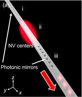
Ryota Katsumi, Masaki Sekino, Takashi Yatsui
Design of an ultra-sensitive and miniaturized diamond NV magnetometer based on a nanocavity structure Journal Article
In: Japanese Journal of Applied Physics, vol. 61, no. 8, pp. 082004, 2022.
Abstract | Links | BibTeX | タグ: Diamond
@article{katsumi22sensor,

title = {Design of an ultra-sensitive and miniaturized diamond NV magnetometer based on a nanocavity structure},

author = {Ryota Katsumi and Masaki Sekino and Takashi Yatsui},

doi = {10.35848/1347-4065/ac7e10},

year  = {2022},

date = {2022-07-05},

urldate = {2022-07-05},

journal = {Japanese Journal of Applied Physics},

volume = {61},

number = {8},

pages = {082004},

abstract = {Ensembles of nitrogen-vacancy (NV) centers in diamond allow for the potential realization of sensitive magnetometers by leveraging their excellent spin properties. However, NV-based magnetometers are limited by their experimental magnetic field sensitivity owing to inefficient photon collection. Moreover, they are disadvantageous for reduced spatial resolution and excessive excitation power. To overcome these issues, we propose ultra-sensitive diamond magnetometers based on nanocavities. The device structure can attain high collection efficiencies and enhance the photon emission intensity of the NV ensemble. This device can allow the efficient photon collection even when considering the positional distribution of the NV centers. Our theoretical analysis indicated that the minimum expected sensitivity is 60 fT/√Hz. Proposed design can achieve volume-normalized sensitivity of 0.92 aT/√(Hz/cm3) along with a required power of 7 μW, both of which are superior to those of bulk diamond. The proposed approach offers a promising route toward highly sensitive and energy-efficient magnetometers.},

keywords = {Diamond},

pubstate = {published},

tppubtype = {article}

}

Ryuichi Hirota, Toru Murayama, Ryota Katsumi, Tokuhisa Kawawaki, Shin Yabukami, Ryuji Igarashi, Yuichi Negishi, Moriaki Kusakabe, Masaki Sekino, Takashi Yatsui, Akihiro Kuwahata
Virus Detection using Second Harmonics of Magnetic Nanoparticles Journal Article
In: IEEJ TRANSACTIONS ON ELECTRICAL AND ELECTRONIC ENGINEERING, vol. 17, iss. 8, pp. 1228-1230, 2022.
Abstract | Links | BibTeX | タグ: SHG, Virus Detection
@article{SHvirus,

title = {Virus Detection using Second Harmonics of Magnetic Nanoparticles},

author = {Ryuichi Hirota and Toru Murayama and Ryota Katsumi and Tokuhisa Kawawaki and Shin Yabukami and Ryuji Igarashi and Yuichi Negishi and Moriaki Kusakabe and Masaki Sekino and Takashi Yatsui and Akihiro Kuwahata},

doi = {10.1002/tee.23613},

year  = {2022},

date = {2022-04-12},

urldate = {2022-04-12},

journal = {IEEJ TRANSACTIONS ON ELECTRICAL AND ELECTRONIC ENGINEERING},

volume = {17},

issue = {8},

pages = {1228-1230},

abstract = {Virus detection methods based on the nonlinear magnetic response of magnetic nanoparticles have been investigated, and magnetic detection methods using the third harmonic have been widely applied on account of their high sensitivity, short measurement-time, and low cost. In this letter, we propose a virus detection method using the second harmonics to improve the signal intensity. We find that the signal to noise ratio of the second harmonic is approximately three times higher than that of the third harmonic. A comparison of the ratio of the second harmonic to the fourth harmonic (R24) and the ratio of the third harmonic to the fifth harmonic (R35) shows that R24 is more sensitive to identifying changes in virus concentration. Our proposed method has the potential to be utilized for rapid screening on virus detection.},

keywords = {SHG, Virus Detection},

pubstate = {published},

tppubtype = {article}

}
2021
Kiyoshi Yatsui, Chihiro Yamada, Yuta Yoshida, Takashi Yatsui
Improving sound of clarinet by coating lacquerware (Wajima-nuri) Journal Article
In: Japanese Journal of Applied Physics, vol. 60, no. 10, pp. 107002, 2021.
Abstract | Links | BibTeX | タグ: Wajima-nuri
@article{clarinet,

title = {Improving sound of clarinet by coating lacquerware (Wajima-nuri)},

author = {Kiyoshi Yatsui and Chihiro Yamada and Yuta Yoshida and Takashi Yatsui},

doi = {10.35848/1347-4065/ac26e4},

year  = {2021},

date = {2021-10-08},

urldate = {2021-10-08},

journal = {Japanese Journal of Applied Physics},

volume = {60},

number = {10},

pages = {107002},

abstract = {Thick films of lacquers by Wajima-nuri were coated only on a barrel and a bell of a clarinet. Significant change of sound characteristics has been observed on the frequency spectra analyzed by FFT. For octave below on A3 (220 Hz), the resonant peaks appear in 8 ~ 10 kHz only coated both on the outer and inner surfaces. For octave above on A5 (880 Hz), dissonances found before the coating disappeared by the coating. The half width of the resonant peaks becomes narrower, resulting in the sharp sounds after being Wajima-nuri. At 15 kHz ~ 20 kHz, the width of the peaks becomes sharp, and the sound pressures are extraordinarily strong if coated on both surfaces. All peaks of sound pressures were shifted to higher frequencies by Wajima-nuri. The improvement of sound characteristics is most effective coated on both inside and outside the barrel and bell of clarinet.},

keywords = {Wajima-nuri},

pubstate = {published},

tppubtype = {article}

}
Zhiyu Wang, Ya‐Lun Ho, Tun Cao, Takashi Yatsui, Jean‐Jacques Delaunay
In: Advanced Functional Materials, 2021.
Abstract | Links | BibTeX | タグ: Selected, Tamm state
@article{advfunmat21,

title = {High‐Q and Tailorable Fano Resonances in a One‐Dimensional Metal‐Optical Tamm State Structure: From a Narrowband Perfect Absorber to a Narrowband Perfect Reflector},

author = {Zhiyu Wang and Ya‐Lun Ho and Tun Cao and Takashi Yatsui and Jean‐Jacques Delaunay},

doi = {10.1002/adfm.202102183},

year  = {2021},

date = {2021-04-19},

urldate = {2021-04-19},

journal = {Advanced Functional Materials},

abstract = {Fano resonances giving rise to a rich variety of asymmetric spectral shapes have been investigated in optical nanostructures with multidimensional configurations. However, 1D nanostructure realizing Fano resonances with well‐controlled spectral shapes are yet to be demonstrated. Here, the authors present both numerically and experimentally a 1D nanostructure exhibiting rich Fano resonances induced by interference between a lossy background (continuum) provided by a metal thin film and a discrete optical Tamm state (OTS). A drastic change in the Fano line shape occurs from a narrowband perfect absorber into a narrowband perfect reflector by controlling the metal thin film. Independent from the metal‐related Fano profile, the OTS component determines the resonance frequency and guarantees a sharp resonance (with quality factors over 1000) on the flat mirror background. Taking advantage of its high‐Q property, the structure can be developed into a dispersion device with subnanometer spectral resolution, which even enables a direct imaging of spectral information of molecular fingerprint. The authors believe that this work not only demonstrates a planar nanostructure with versatile Fano resonances for various applications but also provides physical insights into how a metal thin film can induce and significantly affect the Fano resonances in 1D optical resonators.},

keywords = {Selected, Tamm state},

pubstate = {published},

tppubtype = {article}

}
Takashi Yatsui, Felix Brandenburg, Benjamin Leuschel, Olivier Soppera
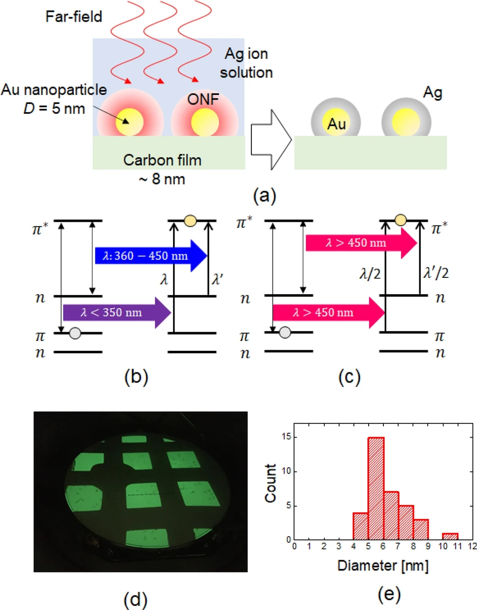
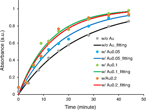
Synthesis of silver nanostructure on gold nanoparticle using near field assisted second harmonic generation Journal Article
In: Scientific Reports, vol. 11, pp. 5642, 2021.
Abstract | Links | BibTeX | タグ: First, Nanophotonic fabrication, Near-field effect, SHG
@article{ag21,

title = {Synthesis of silver nanostructure on gold nanoparticle using near field assisted second harmonic generation},

author = {Takashi Yatsui and Felix Brandenburg and Benjamin Leuschel and Olivier Soppera},

doi = {10.1038/s41598-021-84944-w},

year  = {2021},

date = {2021-03-11},

urldate = {2021-03-11},

journal = {Scientific Reports},

volume = {11},

pages = {5642},

abstract = {By using gold (Au) nanoparticles (NPs) as an optical near-field source under far-field illumination in combination with a silver (Ag) ion solution containing a photoinitiator, we coated Ag on Au NPs using a near-field (NF)-assisted process. We evaluated the change in the size of the NPs using transmission electron microscopy. Evaluation of the synthesized Ag volume over illumination power confirmed the squared power dependence of the NP volume with illumination using 808 nm light, i.e., a wavelength longer than the absorption edge wavelength of the photoinitiator molecules. The rate of volume increase was much lower than the plasmonic field enhancement effect. Therefore, the squared power dependency of the volume increase using a wavelength longer than the absorption edge wavelength originated from NF-assisted second-harmonic generation and the resulting excitation.},

keywords = {First, Nanophotonic fabrication, Near-field effect, SHG},

pubstate = {published},

tppubtype = {article}

}
Takahiro Kitaizumi, Akihiro Kuwahata, Kota Saichi, Takumi Sato, Ryuji Igarashi, Takeshi Ohshima, Yuta Masuyama, Takayuki Iwasaki, Mutsuko Hatano, Fedor Jelezko, Moriaki Kusakabe, Takashi Yatsui, Masaki Sekino
In: IEEE Transactions on Magnetics, vol. 57, no. 2, pp. 5100405, 2021.
Abstract | Links | BibTeX | タグ: NV center
@article{kitaizumi20,

title = {Magnetic field generation system of the magnetic probe with diamond quantum sensor and ferromagnetic materials for the detection of sentinel lymph nodes with magnetic nanoparticles},

author = {Takahiro Kitaizumi and Akihiro Kuwahata and Kota Saichi and Takumi Sato and Ryuji Igarashi and Takeshi Ohshima and Yuta Masuyama and Takayuki Iwasaki and Mutsuko Hatano and Fedor Jelezko and Moriaki Kusakabe and Takashi Yatsui and Masaki Sekino},

doi = {10.1109/TMAG.2020.3009334},

year  = {2021},

date = {2021-01-21},

journal = {IEEE Transactions on Magnetics},

volume = {57},

number = {2},

pages = {5100405},

abstract = {We have developed the magnetic probe with a diamond quantum sensor and electromagnetic coils to detect sentinel lymph nodes (SLNs), as the medical application of diamond quantum sensing. The probe magnetizes magnetic nanoparticles (MNPs) accumulated in SLNs and detect the magnetic fields of magnetized MNPs. In this study. We designed a ferromagnetic core that has a unique shape and optimized the magnetic field generation system for improving the detection performance, such as the magnetic sensitivity and detectable distance. The proposed magnetic core enhances an excitation magnetic field strength at a longer distance and suppresses a bias field strength at a location of the diamond quantum sensor. The increment of the excitation field is approximately 370% and the decrement of the bias field is approximately 45%. In addition to the proposed magnetic core, even applying a cancellation coil, the excitation field strength is ten-fold compared with the coil only structure, suggesting the larger magnetization of MNPs generates the large magnetic field for longer detectable distance.},

keywords = {NV center},

pubstate = {published},

tppubtype = {article}

}
2020
Takashi Yatsui, Yuki Nakamura, Yosuke Suzuki, Tatsuki Morimoto, Yuma Kato, Muneaki Yamamoto, Tomoko Yoshida, Wataru Kurashige, Nobuyuki Shimizu, Yuichi Negishi, Kenji Iida, Katsuyuki Nobusada
Increase in CO2 reduction rate via optical near-field effect Journal Article
In: Journal of Nanophotonics, vol. 14, no. 4, pp. 046011, 2020.
Abstract | Links | BibTeX | タグ: CO2 reduction, Near-field effect
@article{CO2reduction,

title = {Increase in CO2 reduction rate via optical near-field effect},

author = {Takashi Yatsui and Yuki Nakamura and Yosuke Suzuki and Tatsuki Morimoto and Yuma Kato and Muneaki Yamamoto and Tomoko Yoshida and Wataru Kurashige and Nobuyuki Shimizu and Yuichi Negishi and Kenji Iida and Katsuyuki Nobusada},

doi = {10.1117/1.JNP.14.046011},

year  = {2020},

date = {2020-11-27},

journal = {Journal of Nanophotonics},

volume = {14},

number = {4},

pages = {046011},

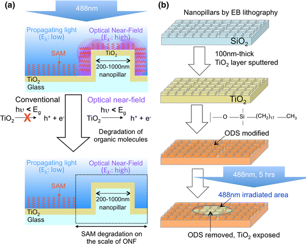
abstract = {To reduce the effects of global warming, visible and near-infrared light must be used more efficiently. Deep ultraviolet light (8 eV) is required for the direct dissociation of CO2 by light; however, the introduction of a metal complex has made it possible to realize CO2 reduction with visible light. We demonstrate that the optical near field (ONF) can increase the CO2 reduction rate. For this, we used gold clusters, because they can be a suitable source for ONFs, as their size and density can be controlled by the number of gold atoms. By attaching a metal complex near gold clusters with diameters of 1.0 to 1.3 nm, we confirm that the reduction rate of CO2 to CO increased by 1.5 to 2.1 times. The gold clusters were sufficiently small; therefore, there was no plasmonic resonant peak or heat generation. Because the near-field effect is based on a photochemical reaction, it can be applied to other metal complexes used in CO2 reduction, and it has other applications such as water splitting and water purification.},

keywords = {CO2 reduction, Near-field effect},

pubstate = {published},

tppubtype = {article}

}

Sarath Raman Nair, Lachlan J. Rogers, Xavier Vidal, Reece P. Roberts, Hiroshi Abe, Takeshi Ohshima, Takashi Yatsui, Andrew D. Greentree, Jan Jeske, Thomas Volz
Amplification by stimulated emission of nitrogen-vacancy centres in a diamond-loaded fibre cavity Journal Article
In: Nanophotonics, vol. 9, no. 15, pp. 4505-4518, 2020.
Abstract | Links | BibTeX | タグ: Near-field etching, NV center
@article{amp20,

title = {Amplification by stimulated emission of nitrogen-vacancy centres in a diamond-loaded fibre cavity},

author = {Sarath Raman Nair and Lachlan J. Rogers and Xavier Vidal and Reece P. Roberts and Hiroshi Abe and Takeshi Ohshima and Takashi Yatsui and Andrew D. Greentree and Jan Jeske and Thomas Volz},

doi = {10.1515/nanoph-2020-0305},

year  = {2020},

date = {2020-11-01},

urldate = {2020-11-01},

journal = {Nanophotonics},

volume = {9},

number = {15},

pages = {4505-4518},

abstract = {Laser threshold magnetometry using the negatively charged nitrogen-vacancy (NV−) centre in diamond as a gain medium has been proposed as a technique to dramatically enhance the sensitivity of room-temperature magnetometry. We experimentally explore a diamond-loaded open tunable fibre-cavity system as a potential contender for the realisation of lasing with NV− centres. We observe amplification of the transmission of a cavity-resonant seed laser at 721 nm when the cavity is pumped at 532 nm and attribute this to stimulated emission. Changes in the intensity of spontaneously emitted photons accompany the amplification, and a qualitative model including stimulated emission and ionisation dynamics of the NV− centre captures the dynamics in the experiment very well. These results highlight important considerations in the realisation of an NV− laser in diamond.},

keywords = {Near-field etching, NV center},

pubstate = {published},

tppubtype = {article}

}
Chih-Zong Deng, Ya-Lun Ho, J. Kenji Clark, Takashi Yatsui, Jean-Jacques Delaunay
Light Switching with a Metal-Free Chiral-Sensitive Metasurface at Telecommunication Wavelengths Journal Article
In: ACS Photonics, vol. 7, no. 10, pp. 2915–2922, 2020.
Abstract | Links | BibTeX | タグ: Nanophotonic device, Near-field effect
@article{LightSwitching,

title = {Light Switching with a Metal-Free Chiral-Sensitive Metasurface at Telecommunication Wavelengths},

author = {Chih-Zong Deng and Ya-Lun Ho and J. Kenji Clark and Takashi Yatsui and Jean-Jacques Delaunay},

doi = {10.1021/acsphotonics.0c01377},

year  = {2020},

date = {2020-10-12},

urldate = {2020-10-12},

journal = {ACS Photonics},

volume = {7},

number = {10},

pages = {2915–2922},

abstract = {Controlling the direction of light propagation, or light switching, enables the addressing of individual optical elements in high-density and complex photonic integrated devices. Light switching is therefore crucial to the development of photonic/plasmonic integrated circuits. Chiral-sensitive metasurfaces using metallic nanostructures have been used to realize light switching by coupling incident light of different spins to surface plasmon polaritons propagating in different directions. However, surface plasmon polaritons-based devices suffer from short propagation lengths and narrow resonance wavelength ranges resulting from ohmic losses in their metal layers. Bloch surface waves can be seen as a metal-free analogy to surface plasmon polaritons with superior properties such as low propagation losses and wide operating wavelength ranges. Here, we demonstrate a metal-free chiral-sensitive Bloch-surface-wave switching circuit consisting of a carefully arranged array of U-shaped apertures, guiding slabs, and grating couplers. By engineering the amplitude and phase of the Bloch surface wave to achieve spin-controlled unidirectional coupling, control of the propagation direction of the Bloch surface waves is realized. Very high directional selectivity is reported at the telecommunications wavelength of 1550 nm, both theoretically at 23 dB and experimentally at 13.5 dB. The ability to realize spin-controlled light switching on a chip at telecommunications wavelengths using metal-free chiral-sensitive metasurfaces should benefit the development of low-loss on-chip photonic integrated devices.},

keywords = {Nanophotonic device, Near-field effect},

pubstate = {published},

tppubtype = {article}

}
Kiyoshi Yatsui, Hidehiko Asaoka, Yuta Yoshida, Takashi Yatsui
Change of sound characteristics of yidaki (didgeridoo) coated with thick films of lacquer (Wajima-nuri) Journal Article
In: Japanese Journal of Applied Physics, vol. 59, no. 7, pp. 077002, 2020.
Abstract | Links | BibTeX | タグ: Wajima-nuri
@article{Yatsui_2020,

title = {Change of sound characteristics of yidaki (didgeridoo) coated with thick films of lacquer (Wajima-nuri)},

author = {Kiyoshi Yatsui and Hidehiko Asaoka and Yuta Yoshida and Takashi Yatsui},

doi = {10.35848/1347-4065/ab9277},

year  = {2020},

date = {2020-06-01},

urldate = {2020-06-01},

journal = {Japanese Journal of Applied Physics},

volume = {59},

number = {7},

pages = {077002},

publisher = {IOP Publishing},

abstract = {Thick films of lacquers were coated by Wajima-nuri on a yidaki (didgeridoo), a woodwind instrument loved by indigenous Australians from ancient times. An investigation of frequency spectra of fast Fourier transform before and after the coating revealed a significant enhancement of sound pressure from the yidaki coated by Wajima-nuri, particularly in the low-frequency region of 500 Hz–1 kHz. All peaks of the sound pressures were shifted to higher frequencies by the Wajima-nuri. The improvement of sound characteristics was greater by Wajima-nuri both inside and outside the yidaki than by Wajima-nuri on the outside only. It might have been due to the fact that the lacquers soaked through the perforated holes and cracks inherent to the original yidaki. Urushiol in lacquers tends to solidify by oxidative polymerization, which resulted in a smooth surface that suppressed the turbulence of the air breathed. These results could be useful for other musical instruments.},

keywords = {Wajima-nuri},

pubstate = {published},

tppubtype = {article}

}
Akihiro Kuwahata, Takahiro Kitaizumi, Kota Saichi, Takumi Sato, Ryuji Igarashi, Takeshi Ohshima, Yuta Masuyama, Takayuki Iwasaki, Mutsuko Hatano, Fedor Jelezko, Moriaki Kusakabe, Takashi Yatsui, Masaki Sekino
Magnetometer with nitrogen-vacancy center in a bulk diamond for detecting magnetic nanoparticles in biomedical applications Journal Article
In: Scientific Reports, vol. 10, pp. 2483, 2020.
Abstract | Links | BibTeX | タグ: Diamond, NV center
@article{Kuwahata2020,

title = {Magnetometer with nitrogen-vacancy center in a bulk diamond for detecting magnetic nanoparticles in biomedical applications},

author = {Akihiro Kuwahata and Takahiro Kitaizumi and Kota Saichi and Takumi Sato and Ryuji Igarashi and Takeshi Ohshima and Yuta Masuyama and Takayuki Iwasaki and Mutsuko Hatano and Fedor Jelezko and Moriaki Kusakabe and Takashi Yatsui and Masaki Sekino},

url = {https://www.altmetric.com/details/75906559},

doi = {10.1038/s41598-020-59064-6},

year  = {2020},

date = {2020-02-01},

journal = {Scientific Reports},

volume = {10},

pages = {2483},

publisher = {Springer Nature},

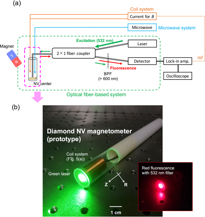
abstract = {We developed a novel magnetometer that employs negatively charged nitrogen-vacancy (NV−) centers in diamond, to detect the magnetic field generated by magnetic nanoparticles (MNPs) for biomedical applications. The compact probe system is integrated into a fiber-optics platform allowing for a compact design. To detect signals from the MNPs effectively, we demonstrated, for the first time, the application of an alternating current (AC) magnetic field generated by the excitation coil of several hundred microteslas for the magnetization of MNPs in diamond quantum sensing. In the lock-in detection system, the minimum detectable AC magnetic field (at a frequency of 1.025 kHz) was approximately 57.6 nT for one second measurement time. We were able to detect the micromolar concentration of MNPs at distances of a few millimeters. These results indicate that the magnetometer with the NV− centers can detect the tiny amounts of MNPs, thereby offering potential for future biomedical applications.},

keywords = {Diamond, NV center},

pubstate = {published},

tppubtype = {article}

}
2019
Naoya Tate, Takashi Yatsui
Visible light-induced thymine dimerisation based on large localised field gradient by non-uniform optical near-field Journal Article
In: Scientific Reports, vol. 9, pp. 18383, 2019.
Abstract | Links | BibTeX | タグ: DNA, Near-field effect, Non-uniform optical near field
@article{tate2019,

title = {Visible light-induced thymine dimerisation based on large localised field gradient by non-uniform optical near-field},

author = {Naoya Tate and Takashi Yatsui},

doi = {10.1038/s41598-019-54661-6},

year  = {2019},

date = {2019-12-01},

journal = {Scientific Reports},

volume = {9},

pages = {18383},

publisher = {Springer Nature},

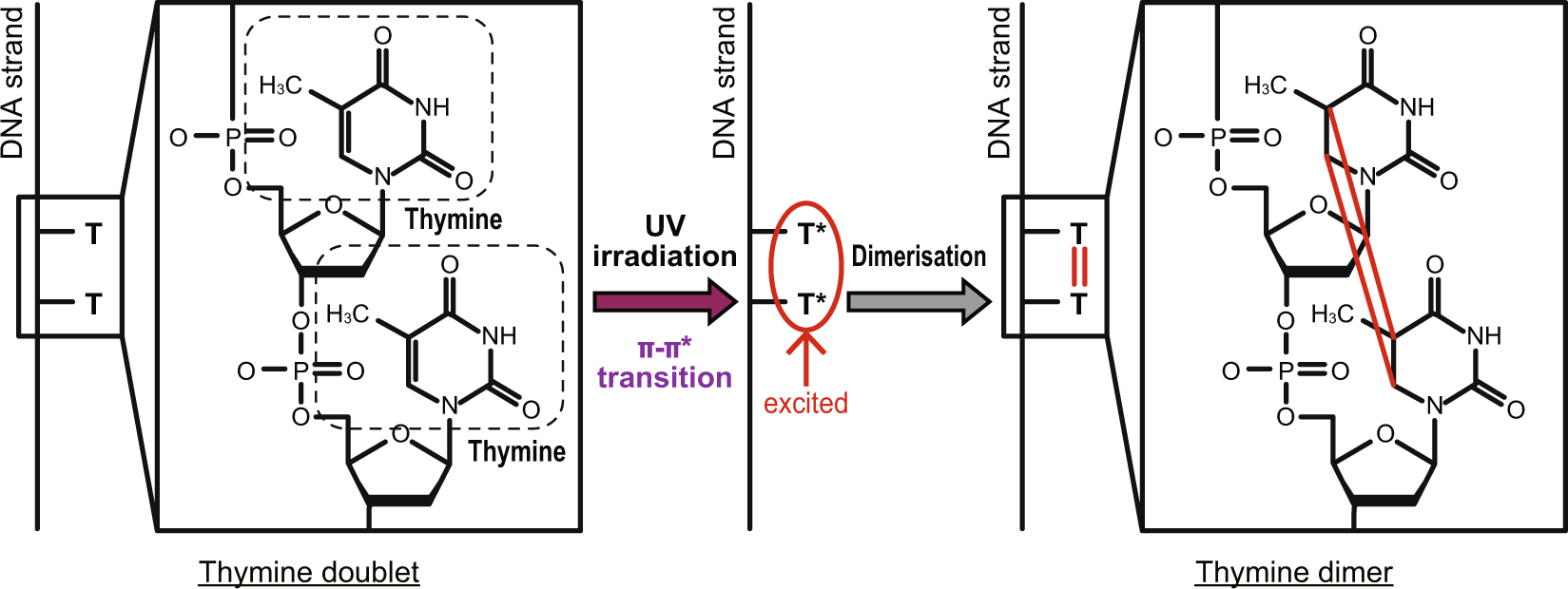
abstract = {The localised excitations of several molecular reactions utilising optical irradiation have been studied in the field of molecular physics. In particular, deoxyribonucleic acid (DNA) strands organise the genetic information of all living matter. Therefore, artificial methods for freely controlling reactions using only light irradiation are highly desirable for reactions of these strands; this in regard with artificial protein synthesis, regional genetic curing, and stochastic analysis of several genetic expressions. Generally, DNA strands have strong absorption features in the deep ultra-violet (DUV) region, which are related to the degradation and reconstruction of the strand bonding structures. However, irradiation by DUV light unavoidably induces unintended molecular reactions which can damage and break the DNA strands. In this paper, we report a photo-induced molecular reaction initiated by the irradiation of DNA strands with visible light. We utilised photo-dissociation from the vibrational levels induced by non-uniform optical near-fields surrounding nanometric Au particles to which DNA strands were attached. The results were experimentally observed by a reduction in the DUV absorbance of the DNA strands during irradiation. There was a much higher yield of molecular reactions than expected due to the absorbance of visible light, and no defects were caused in the DNA strands.},

keywords = {DNA, Near-field effect, Non-uniform optical near field},

pubstate = {published},

tppubtype = {article}

}
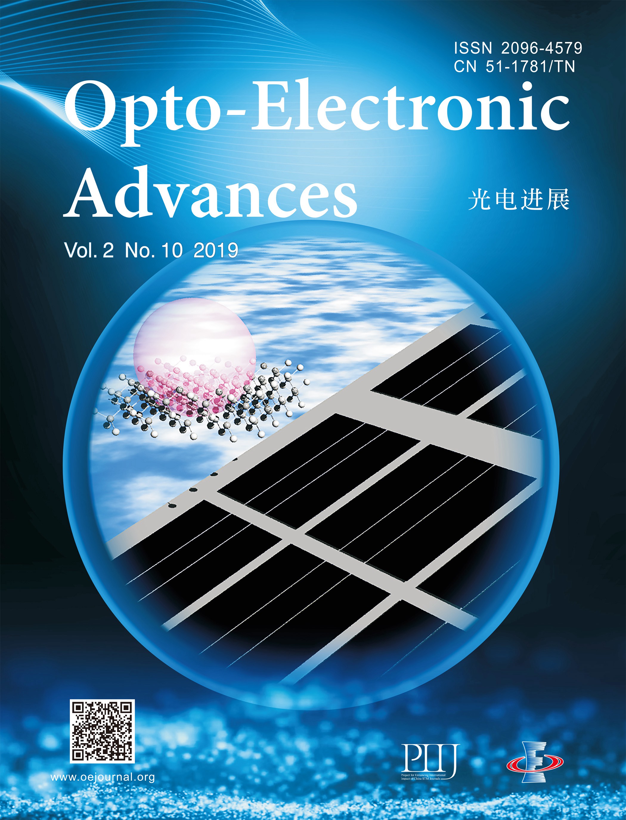
Takashi Yatsui
Recent improvement of silicon absorption in opto-electric devices Journal Article
In: Opto-Electronic Advances, vol. 2, no. 10, pp. 190023, 2019, (review article, selected as cover story).
Abstract | Links | BibTeX | タグ: Direct wave-vector excitation, First, First principle calculation, Indirect band gap, Near-field effect, Plasmon, Review, Si
@article{OEA_RefItem:1,

title = {Recent improvement of silicon absorption in opto-electric devices},

author = {Takashi Yatsui},

doi = {10.29026/oea.2019.190023},

year  = {2019},

date = {2019-10-01},

urldate = {2019-10-01},

journal = {Opto-Electronic Advances},

volume = {2},

number = {10},

pages = {190023},

publisher = {OEA},

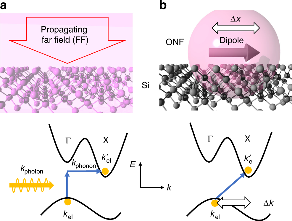
abstract = {Silicon dominates the contemporary electronic industry. However, being an indirect band-gap material, it is a poor absorber of light, which decreases the efficiency of Si-based photodetectors and photovoltaic devices. This review highlights recent studies performed towards improving the optical absorption of Si. A summary of recent theoretical approaches based on the first principle calculation has been provided. It is followed by an overview of recent experimental approaches including scattering, plasmon, hot electron, and near-field effects. The article concludes with a perspective on the future research direction of Si-based photodetectors and photovoltaic devices.},

note = {review article, selected as cover story},

keywords = {Direct wave-vector excitation, First, First principle calculation, Indirect band gap, Near-field effect, Plasmon, Review, Si},

pubstate = {published},

tppubtype = {article}

}
Takashi Yatsui, Syunsuke Okada, Tatsuya Takemori, Takumi Sato, Kota Saichi, Tatsuro Ogamoto, Shohei Chiashi, Shigeo Maruyama, Masashi Noda, Kazuhiro Yabana, Kenji Iida, Katsuyuki Nobusada
Enhanced photo-sensitivity in a Si photodetector using a near-field assisted excitation Journal Article
In: Communications Physics, vol. 2, pp. 62, 2019.
Abstract | Links | BibTeX | タグ: Direct wave-vector excitation, First, Selected, Si photodetector
@article{yatsui2019Si,

title = {Enhanced photo-sensitivity in a Si photodetector using a near-field assisted excitation},

author = {Takashi Yatsui and Syunsuke Okada and Tatsuya Takemori and Takumi Sato and Kota Saichi and Tatsuro Ogamoto and Shohei Chiashi and Shigeo Maruyama and Masashi Noda and Kazuhiro Yabana and Kenji Iida and Katsuyuki Nobusada},

doi = {10.1038/s42005-019-0173-1},

year  = {2019},

date = {2019-06-01},

journal = {Communications Physics},

volume = {2},

pages = {62},

publisher = {Springer Nature},

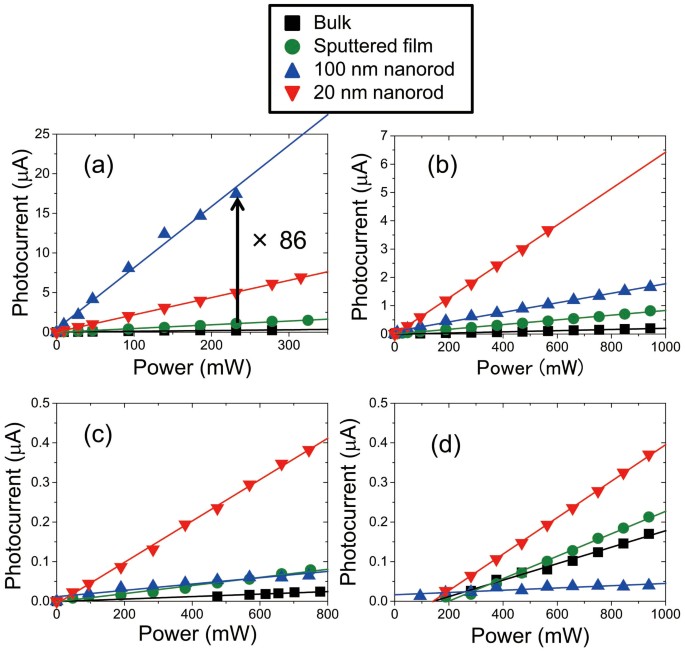
abstract = {Silicon is an indispensable material in electric device technology. However, Si is an indirect bandgap material; therefore, its excitation efficiency, which requires phonon assistance, is low under propagating far-field light. To improve the excitation efficiency, herein we performed optical near-field excitation, which is confined in a nano-scale, where the interband transitions between different wave numbers are excited according to the uncertainty principle; thus, optical near-field can directly excite the carrier in the indirect bandgap. To evaluate the effect of optical near-field confined in a nano-scale, we fabricate the lateral Si p-n junction with Au nanoparticles as sources to generate the field confinement. We observed a 47.0 % increase in the photo-sensitivity rate. In addition, by using the thin lateral p-n junction, which eliminates the far-field excitation, we confirmed a 42.3 % increase in the photo-sensitivity rate.},

keywords = {Direct wave-vector excitation, First, Selected, Si photodetector},

pubstate = {published},

tppubtype = {article}

}
Takashi Yatsui, Yusuke Nakahira, Yuki Nakamura, Tatsuki Morimoto, Yuma Kato, Muneaki Yamamoto, Tomoko Yoshida, Kenji Iida, Katsuyuki Nobusada
Realization of red shift of absorption spectra using optical near-field effect Journal Article
In: Nanotechnology, vol. 30, no. 34, pp. 34LT02, 2019.
Abstract | Links | BibTeX | タグ: CO2 reduction, First, Near-field effect
@article{Yatsui_2019,

title = {Realization of red shift of absorption spectra using optical near-field effect},

author = {Takashi Yatsui and Yusuke Nakahira and Yuki Nakamura and Tatsuki Morimoto and Yuma Kato and Muneaki Yamamoto and Tomoko Yoshida and Kenji Iida and Katsuyuki Nobusada},

doi = {10.1088/1361-6528/ab2092},

year  = {2019},

date = {2019-06-01},

journal = {Nanotechnology},

volume = {30},

number = {34},

pages = {34LT02},

publisher = {IOP Publishing},

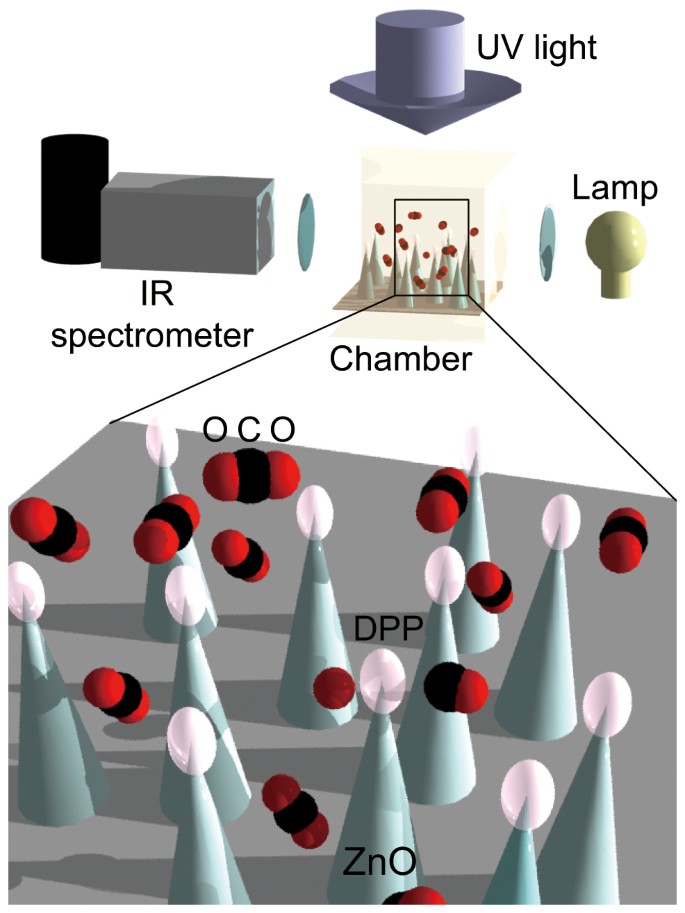
abstract = {In many applications such as CO2 reduction and water splitting, high-energy photons in the ultraviolet region are required to complete the chemical reactions. However, to realize sustainable development, the photon energies utilized must be lower than the absorption edge of the materials including the metal complex for CO2 reduction, the electrodes for water splitting, because of the huge amount of lower energy than the visible region received from the sun. In the previous works, we had demonstrated that optical near-fields (ONFs) could realize chemical reactions, by utilizing photon energies much lower than the absorption edge because of the spatial non-uniformity of the electric field. In this paper, we demonstrate that an ONF can realize the red shift of the absorption spectra of the metal-complex material for photocatalytic reduction. By attaching the metal complex to ZnO nano-crystalline aggregates with nano-scale protrusions, the absorption spectra by using diffuse reflection of the metal complex can be shifted to a longer wavelength by 10.6 nm. The results of computational studies based on a first-principles computational program including the ONF effect provide proof of the increase in the absorption of the metal complex at lower photon energies. Since the near-field assisted field increase improves the carrier excitation in the metal-complex materials, this effect may be universal and it could applicable to CO2 reduction using the other metal-complex materials, as well as to the other photo excitation process including water splitting.},

keywords = {CO2 reduction, First, Near-field effect},

pubstate = {published},

tppubtype = {article}

}
Masashi Noda, Kenji Iida, Maiku Yamaguchi, Takashi Yatsui, Katsuyuki Nobusada
Direct Wave-Vector Excitation in an Indirect-Band-Gap Semiconductor of Silicon with an Optical Near-field Journal Article
In: Phys. Rev. Applied, vol. 11, no. 4, pp. 044053, 2019.
Abstract | Links | BibTeX | タグ: Direct wave-vector excitation, Si
@article{PhysRevApplied.11.044053,

title = {Direct Wave-Vector Excitation in an Indirect-Band-Gap Semiconductor of Silicon with an Optical Near-field},

author = {Masashi Noda and Kenji Iida and Maiku Yamaguchi and Takashi Yatsui and Katsuyuki Nobusada},

doi = {10.1103/PhysRevApplied.11.044053},

year  = {2019},

date = {2019-04-01},

journal = {Phys. Rev. Applied},

volume = {11},

number = {4},

pages = {044053},

publisher = {American Physical Society},

abstract = {In this work, our first-principles calculations reveal that direct wave-vector excitation (i.e., interband transitions between different wavenumbers without phonon assistance) can occur in the indirect-band-gap semiconductor silicon. The wave-vector excitation is successfully induced by irradiation of a silicon thin film with an optical near-field (ONF). As a result, the absorption-band-edge energy Eedge shifts to a lower photon energy of 1.6 eV for ONF excitation from Eedge of 2.1 eV for the conventional excitation by propagating far-field light. The direct wave-vector excitation is caused by the sufficiently large components of wave vectors inherent in the ONF, and thus does not require phonon assistance. For a realistic silicon system, it is clarified that the wave-vector excitations are determined by the energy difference between the valence and conduction bands and occur irrespective of the initial and final wave vectors.},

keywords = {Direct wave-vector excitation, Si},

pubstate = {published},

tppubtype = {article}

}
2018
Felix Brandenburg, Ryosuke Nagumo, Kota Saichi, Kosuke Tahara, Takayuki Iwasaki, Mutsuko Hatano, Fedor Jelezko, Ryuji Igarashi, Takashi Yatsui
Improving the electron spin properties of nitrogen-vacancy centres in nanodiamonds by near-field etching Journal Article
In: Scientific Reports, vol. 8, pp. 15847, 2018.
Abstract | Links | BibTeX | タグ: Diamond, Nanophotonic fabrication, Near-field etching, NV center
@article{2018Felix,

title = {Improving the electron spin properties of nitrogen-vacancy centres in nanodiamonds by near-field etching},

author = {Felix Brandenburg and Ryosuke Nagumo and Kota Saichi and Kosuke Tahara and Takayuki Iwasaki and Mutsuko Hatano and Fedor Jelezko and Ryuji Igarashi and Takashi Yatsui},

doi = {10.1038/s41598-018-34158-4},

year  = {2018},

date = {2018-10-01},

urldate = {2018-10-01},

journal = {Scientific Reports},

volume = {8},

pages = {15847},

publisher = {Springer Nature},

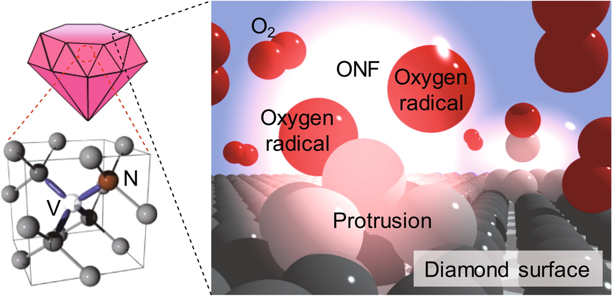
abstract = {The nitrogen-vacancy (NV) centre in diamond is a promising candidate for quantum computing applications and magnetic sensing applications, because it is an atomic-scale defect with stable coherence time (T2) and reliable accessibility at room temperature. We demonstrated a method for improving the NV spin properties (the full width half maximum (FWHM) value of the magnetic resonance spectrum and T2) through a near-field (NF) etching method under ambient conditions. The NF etching method, based on a He-Cd ultraviolet laser (325 nm), which is longer than the absorption edge of the oxygen molecule, enabled selective removal of defects on the nanodiamond surface. We observed a decrease in the FWHM value close to 15% and an increase in T2 close to 25%. Since our technique can be easily reproduced, a wide range of NV centre applications could be improved, especially magnetic sensing applications. Our results are especially attractive, because they have been obtained under ambient conditions and only require a light source with wavelength slightly above the O2 absorption edge.},

keywords = {Diamond, Nanophotonic fabrication, Near-field etching, NV center},

pubstate = {published},

tppubtype = {article}

}
2017
Takashi Yatsui, Hiroshi Saito, Katsuhiro Nishioka, Benjamin Leuschel, Olivier Soppera, Katsuyuki Nobusada
Effects of a power and photon energy of incident light on near-field etching properties Journal Article
In: Applied Physics A, vol. 123, no. 12, pp. 751, 2017.
Abstract | Links | BibTeX | タグ: First, Nanophotonic fabrication, Near-field etching
@article{2017yatsuiAPA,

title = {Effects of a power and photon energy of incident light on near-field etching properties},

author = {Takashi Yatsui and Hiroshi Saito and Katsuhiro Nishioka and Benjamin Leuschel and Olivier Soppera and Katsuyuki Nobusada},

doi = {10.1007/s00339-017-1361-z},

year  = {2017},

date = {2017-12-01},

journal = {Applied Physics A},

volume = {123},

number = {12},

pages = {751},

publisher = {Springer Nature},

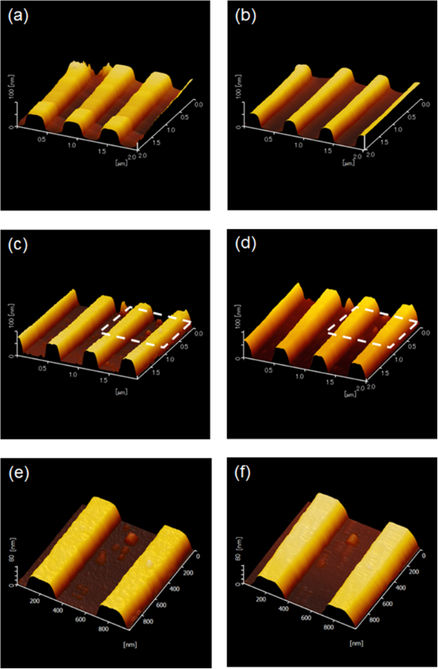
abstract = {We developed a near-field etching technique for realizing an ultra-flat surfaces of various materials and structures. To elucidate the near-field etching properties, we have investigated the effects of power and the photon energy of the incident light. First, we established theoretically that an optical near-field with photon energy lower than the absorption edge of the molecules can induce molecular vibrations. We used nanodiamonds to study the power dependence of the near-field etching properties. From the topological changes of the nanodiamonds, we confirmed the linear-dependence of the etching volume with the incident power. Furthermore, we studied the photon energy dependence using TiO2 nanostriped structures, which revealed that a lower photon energy results in a lower etching rate.},

keywords = {First, Nanophotonic fabrication, Near-field etching},

pubstate = {published},

tppubtype = {article}

}
Takashi Yatsui, Hiroshi Saito, Katsuyuki Nobusada
Angstrom-scale flatness using selective nanoscale etching Journal Article
In: Beilstein Journal of Nanotechnology, vol. 123, pp. 751, 2017.
Abstract | Links | BibTeX | タグ: First, Nanophotonic fabrication, Near-field etching, Wet etching
@article{2017yatsuiBJ,

title = {Angstrom-scale flatness using selective nanoscale etching},

author = {Takashi Yatsui and Hiroshi Saito and Katsuyuki Nobusada},

doi = {10.3762/bjnano.8.217},

year  = {2017},

date = {2017-10-01},

journal = {Beilstein Journal of Nanotechnology},

volume = {123},

pages = {751},

publisher = {Beilstein-Institut.},

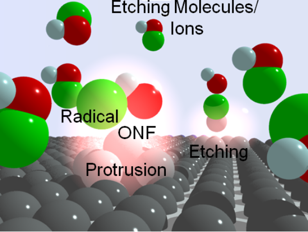
abstract = {The realization of flat surfaces on the angstrom scale is required in advanced devices to avoid loss due to carrier (electron and/or photon) scattering. In this work, we have developed a new surface flattening method that involves near-field etching, where optical near-fields (ONFs) act to dissociate the molecules. ONFs selectively generated at the apex of protrusions on the surface selectively etch the protrusions. To confirm the selective etching of the nanoscale structure, we compared near-field etching using both gas molecules and ions in liquid phase. Using two-dimensional Fourier analysis, we found that near-field etching is an effective way to etch on the scale of less than 10 nm for both wet and dry etching techniques. In addition, near-field dry etching may be effective for the selective etching of nanoscale structures with large mean free path values.},

keywords = {First, Nanophotonic fabrication, Near-field etching, Wet etching},

pubstate = {published},

tppubtype = {article}

}
Takashi Yatsui, Maiku Yamaguchi, Katsuyuki Nobusada
Nano-scale chemical reactions based on non-uniform optical near-fields and their applications Journal Article
In: Progress in Quantum Electronics, vol. 55, pp. 166 - 194, 2017, ISSN: 0079-6727, (review article).
Abstract | Links | BibTeX | タグ: Artificial photosynthesis, First, Near-field etching, Non-uniform optical near field, Photodissociation path with two-step excitation, Review, Selected, SHG
@article{YATSUI2017166,

title = {Nano-scale chemical reactions based on non-uniform optical near-fields and their applications},

author = {Takashi Yatsui and Maiku Yamaguchi and Katsuyuki Nobusada},

doi = {10.1016/j.pquantelec.2017.06.001},

issn = {0079-6727},

year  = {2017},

date = {2017-09-01},

journal = {Progress in Quantum Electronics},

volume = {55},

pages = {166 - 194},

abstract = {Interaction between light and materials is essential in the physics underlying all optical devices, including light emitting devices such as light emitting diodes and lasers, photo-voltaic devices, and photo-synthesis systems. The demand for higher light utilization efficiency is becoming increasingly important for advanced optical devices. This is because, when feature size is smaller than the incident light wavelength, photons cannot couple with devices efficiently. In this paper, we review recent progress regarding a unique phenomenon at the nano scale and its applications. First, we summarize the development of light–matter interactions at the nano-scale. Second, we review recent theoretical works focusing on optical near fields in which unique phenomena arise from non-uniform optical fields. We then review several recent developments based on the near-field effect, including artificial photosynthesis and near-field etching for realization of angstrom-scale fattened surfaces. Finally, we discuss the future outlook for these technologies.},

note = {review article},

keywords = {Artificial photosynthesis, First, Near-field etching, Non-uniform optical near field, Photodissociation path with two-step excitation, Review, Selected, SHG},

pubstate = {published},

tppubtype = {article}

}
Felix Brandenburg, Tomohiro Okamoto, Hiroshi Saito, Benjamin Leuschel, Olivier Soppera, Takashi Yatsui
Surface improvement of organic photoresists using a near-field-dependent etching method Journal Article
In: Beilstein Journal of Nanotechnology, vol. 8, pp. 784-788, 2017.
Abstract | Links | BibTeX | タグ: Nanophotonic fabrication, Near-field etching
@article{2017FelixBJ,

title = {Surface improvement of organic photoresists using a near-field-dependent etching method},

author = {Felix Brandenburg and Tomohiro Okamoto and Hiroshi Saito and Benjamin Leuschel and Olivier Soppera and Takashi Yatsui},

doi = {10.3762/bjnano.8.81},

year  = {2017},

date = {2017-04-01},

journal = {Beilstein Journal of Nanotechnology},

volume = {8},

pages = {784-788},

publisher = {Beilstein-Institut.},

abstract = {Surface flattening techniques are extremely important for the development of future electrical and/or optical devices because carrier-scattering losses due to surface roughness severely limit the performance of nanoscale devices. To address the problem, we have developed a near-field etching technique that provides selective etching of surface protrusions, resulting in an atomically flat surface. To achieve finer control, we examine the importance of the wavelength of the near-field etching laser. Using light sources at wavelengths of 325 and 405 nm, which are beyond the absorption edge of the photoresist (310 nm), we compare the resulting cross-sectional etching volumes. The volumes were larger when 325 nm light was employed, i.e., closer to the absorption edge. Although 405 nm light did not cause structural change in the photoresist, a higher reduction of the surface roughness was observed as compared to the 325 nm light. These results indicate that even wavelengths above 325 nm can cause surface roughness improvements without notably changing the structure of the photoresist.},

keywords = {Nanophotonic fabrication, Near-field etching},

pubstate = {published},

tppubtype = {article}

}
2016
Martin Silies, Manfred Mascheck, David Leipold, Heiko Kollmann, Slawa Schmidt, Janos Sartor, Takashi Yatsui, Kokoro Kitamura, Motoichi Ohtsu, Heinz Kalt, Erich Runge, Christoph Lienau
In: Applied Physics B, vol. 8, no. 7, pp. 181, 2016.
Abstract | Links | BibTeX | タグ: localization
@article{2017SilesAPB,

title = {Near-field assisted localization: Effect of size and filling factor of randomly distributed zinc oxide nanoneedles on multiple scattering and localization of light},

author = {Martin Silies and Manfred Mascheck and David Leipold and Heiko Kollmann and Slawa Schmidt and Janos Sartor and Takashi Yatsui and Kokoro Kitamura and Motoichi Ohtsu and Heinz Kalt and Erich Runge and Christoph Lienau},

doi = {10.1007/s00340-016-6456-2},

year  = {2016},

date = {2016-07-01},

journal = {Applied Physics B},

volume = {8},

number = {7},

pages = {181},

publisher = {Springer Nature},

abstract = {We investigate the influence of the diameter and the filling factor of randomly arranged ZnO nanoneedles on the multiple scattering and localization of light in disordered dielectrics. Coherent, ultra-broadband second-harmonic (SH) microscopy is used to probe the spatial localization of light in representative nm-sized ZnO arrays of needles. We observe strong fluctuations of the SH intensity inside different ZnO needle geometries. Comparison of the SH intensity distributions with predictions based on a one-parameter scaling model indicate that SH fluctuations can be taken as a quantitative measure for the degree of localization. Interestingly, the strongest localization signatures are found for densely packed arrays of thin needles with diameters in the range of only 30 nm range, despite the small scattering cross section of these needles. FDTD simulations indicate that in this case coupling of electric near-fields between neighbouring needles governs the localization.},

keywords = {localization},

pubstate = {published},

tppubtype = {article}

}
Takashi Yatsui, Toshiki Tsuboi, Maiku Yamaguchi, Katsuyuki Nobusada, Satoshi Tojo, Fabrice Stehlin, Olivier Soppera, Daniel Bloch
Optically controlled magnetic-field etching on the nano-scale Journal Article
In: Light: Science & Applications, vol. 5, pp. e16054, 2016.
Abstract | Links | BibTeX | タグ: First, Nanophotonic fabrication, Near-field etching, Selected
@article{2016YatsuiLST,

title = {Optically controlled magnetic-field etching on the nano-scale},

author = {Takashi Yatsui and Toshiki Tsuboi and Maiku Yamaguchi and Katsuyuki Nobusada and Satoshi Tojo and Fabrice Stehlin and Olivier Soppera and Daniel Bloch},

url = {https://www.altmetric.com/details/6399772},

doi = {10.1038/lsa.2016.54},

year  = {2016},

date = {2016-03-25},

journal = {Light: Science & Applications},

volume = {5},

pages = {e16054},

publisher = {Springer Nature},

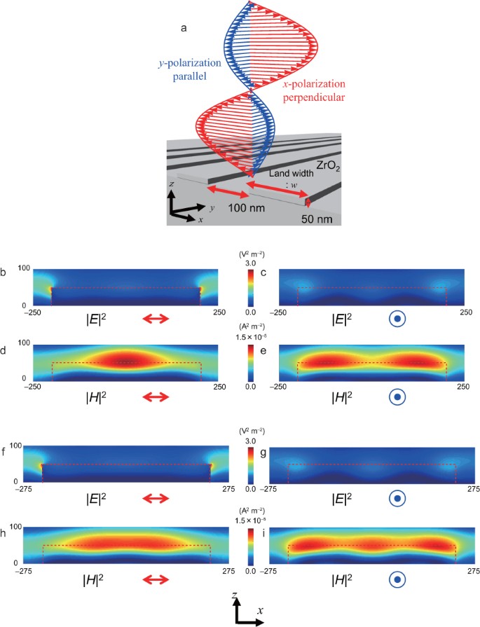
abstract = {Electric and magnetic fields play an important role in both chemical and physical reactions. However, since the coupling efficiency between magnetic fields and electrons is low in comparison with that between electric fields and electrons in the visible wavelength region, the magnetic field is negligible in photo-induced reactions. Here, we performed photo-etching of ZrO2 nano-stripe structures, and identified an etching-property polarisation dependence. Specifically, the etching rate and etched profiles depend on the structure width. To evaluate this polarisation-dependent etching, we performed numerical calculations using a finite-difference time-domain method. Remarkably, the numerical results revealed that the polarisation-dependent etching properties were determined by the magnetic field distributions, rather than the electric field distributions. As nano-scale structures induce a localised magnetic field, the discovery of this etching dependence on the magnetic field is expected to introduce a new perspective on advanced nano-scale structure fabrication.},

keywords = {First, Nanophotonic fabrication, Near-field etching, Selected},

pubstate = {published},

tppubtype = {article}

}
Takashi Yatsui, Kazunori Kuribara, Tsuyoshi Sekitani, Takao Someya, Mamoru Yoshimoto
Temperature-modulated annealing of c-plane sapphire for long-range-ordered atomic steps Journal Article
In: Journal of Physics D: Applied Physics, vol. 49, no. 11, pp. 115302, 2016.
Abstract | Links | BibTeX | タグ: chocolate, First, sapphire, tempering
@article{Yatsui_2016,

title = {Temperature-modulated annealing of c-plane sapphire for long-range-ordered atomic steps},

author = {Takashi Yatsui and Kazunori Kuribara and Tsuyoshi Sekitani and Takao Someya and Mamoru Yoshimoto},

doi = {10.1088/0022-3727/49/11/115302},

year  = {2016},

date = {2016-03-23},

urldate = {2016-03-23},

journal = {Journal of Physics D: Applied Physics},

volume = {49},

number = {11},

pages = {115302},

publisher = {IOP Publishing},

abstract = {High-quality single-crystalline sapphire is used to prepare various semiconductors because of its thermal stability. Here, we applied the tempering technique, which is well known in the production of chocolate, to prepare a sapphire substrate. Surprisingly, we successfully realised millimetre-range ordering of the atomic step of the sapphire substrate. We also obtained a sapphire atomic step with nanometre-scale uniformity in the terrace width and atomic-step height. Such sapphire substrates will find applications in the preparation of various semiconductors and devices.},

keywords = {chocolate, First, sapphire, tempering},

pubstate = {published},

tppubtype = {article}

}
2015
Ryosuke Nagumo, Felix Brandenburg, Anna Ermakova, Fedor Jelezko, Takashi Yatsui
Spectral control of nanodiamond using dressed photon-phonon etching Journal Article
In: Applied Physics A, vol. 121, no. 4, pp. 1335-1339, 2015.
Abstract | Links | BibTeX | タグ: Diamond, Nanophotonic fabrication, Near-field etching, NV center
@article{2015NagumoAPA,

title = {Spectral control of nanodiamond using dressed photon-phonon etching},

author = {Ryosuke Nagumo and Felix Brandenburg and Anna Ermakova and Fedor Jelezko and Takashi Yatsui},

doi = {10.1007/s00339-015-9400-0},

year  = {2015},

date = {2015-12-01},

journal = {Applied Physics A},

volume = {121},

number = {4},

pages = {1335-1339},

publisher = {Springer Nature},

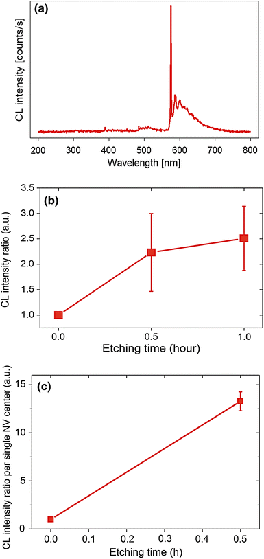
abstract = {The luminescence of a nitrogen-vacancy (NV) center in a nanodiamond (ND) is of great interest because of its features, especially in the field of nanophotonics. When an NV center in an ND is located in the vicinity of the surface, the emission is often disturbed by any surface defects, resulting in non-radiative recombination. In this work, we performed dressed photon-phonon (DPP) etching of the NDs, and found that the size of the NDs decreased, while the cathodoluminescence (CL) intensity increased. We assume that this increase in the CL intensity originates from the removal of the surface protrusions and/or defects by DPP etching.},

keywords = {Diamond, Nanophotonic fabrication, Near-field etching, NV center},

pubstate = {published},

tppubtype = {article}

}
Maiku Yamaguchi, Tadashi Kawazoe, Takashi Yatsui, Motoichi Ohtsu
In: Applied Physics A, vol. 121, no. 4, pp. 1389-1394, 2015.
Abstract | Links | BibTeX | タグ: Annealing
@article{2015YamaguchiAPA,

title = {Spectral properties of a lateral p-n homojunction-structured visible silicon light emitting diode fabricated by dressed-photon-phonon-assisted annealing},

author = {Maiku Yamaguchi and Tadashi Kawazoe and Takashi Yatsui and Motoichi Ohtsu},

doi = {10.1007/s00339-015-9432-5},

year  = {2015},

date = {2015-12-01},

journal = {Applied Physics A},

volume = {121},

number = {4},

pages = {1389-1394},

publisher = {Springer Nature},

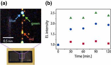
abstract = {We developed a visible silicon light-emitting diode (Si-LED) with a lateral p-n homojunction using dressed-photon-phonon (DPP)-assisted annealing. The lateral p-n homojunction was fabricated in order to decrease the absorption loss inherent in light emission with a photon energy higher than the band-gap energy of the material. The fabricated Si-LED emitted light in the entire visible range, including the three primary colors. The light extraction efficiency of the Si-LED was estimated to be 7.8 times higher than that of a conventional LED structure with a vertical p-n homojunction. Owing to the efficient light extraction, we clearly observed two novel features in the electroluminescence (EL) spectrum: a nonlinear increase in the EL intensity with the injected forward current, and an emission peak at 2.7 eV, at which there is no singular point in the electronic structure. From these features, we concluded that the EL from the Si-LED originated from the phonon-assisted radiative recombination of carriers with much higher energy than that of the bottom of the conduction band, via DPPs.},

keywords = {Annealing},

pubstate = {published},

tppubtype = {article}

}
Wataru Nomura, Takashi Yatsui, Tadashi Kawazoe, Naoya Tate, Motoichi Ohtsu
High-speed flattening of crystallized glass substrates by dressed-photon-phonon etching Journal Article
In: Applied Physics A, vol. 121, no. 4, pp. 1403-1407, 2015.
Abstract | Links | BibTeX | タグ: Nanophotonic fabrication, Near-field etching
@article{2015NomuraAPA,

title = {High-speed flattening of crystallized glass substrates by dressed-photon-phonon etching},

author = {Wataru Nomura and Takashi Yatsui and Tadashi Kawazoe and Naoya Tate and Motoichi Ohtsu},

doi = {10.1007/s00339-015-9466-8},

year  = {2015},

date = {2015-12-01},

journal = {Applied Physics A},

volume = {121},

number = {4},

pages = {1403-1407},

publisher = {Springer Nature},

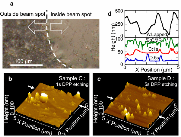
abstract = {Dressed-photon-phonon (DPP) etching is a non-contact flattening technology that realizes ultra-flat surfaces and has been reported to achieve an arithmetic mean surface roughness, R a, on the order of 0.1 nm in various materials, such as fused silica, plastic films, and GaN crystal. In this study, we successfully flattened the surface of a crystallized glass substrate in several seconds using laser light with a higher power density than that used in previous studies. The target substrate had an initial appearance similar to frosted glass, with an R a of 92.5 nm. We performed DPP etching under a Cl2 atmosphere using a CW laser with a wavelength of 532 nm, a power of 8 W, and a spot diameter of 0.2 mm. After 1 s of processing, we obtained a flat surface with an R a of 5.00 nm. This surface roughness equaled or surpassed that of a substrate flattened by conventional chemical mechanical polishing, with an R a of 5.77 nm. Through the detailed analysis of atomic force microscopic images, we found the DPP etching resulted in the smaller standard deviation of the height difference than CMP in the smaller lateral size than 50 nm.},

keywords = {Nanophotonic fabrication, Near-field etching},

pubstate = {published},

tppubtype = {article}

}
Maiku Yamaguchi, Katsuyuki Nobusada, Takashi Yatsui
Nonlinear optical response induced by a second-harmonic electric-field component concomitant with optical near-field excitation Journal Article
In: Phys. Rev. A, vol. 92, no. 4, pp. 043809, 2015.
Abstract | Links | BibTeX | タグ: Non-uniform optical near field, Selected, SHG
@article{PhysRevA.92.043809,

title = {Nonlinear optical response induced by a second-harmonic electric-field component concomitant with optical near-field excitation},

author = {Maiku Yamaguchi and Katsuyuki Nobusada and Takashi Yatsui},

doi = {10.1103/PhysRevA.92.043809},

year  = {2015},

date = {2015-10-01},

journal = {Phys. Rev. A},

volume = {92},

number = {4},

pages = {043809},

publisher = {American Physical Society},

abstract = {Electron dynamics excited by an optical near field (ONF) in a two-dimensional quantum dot model was investigated by solving a time-dependent Schrödinger equation. It was found that the ONF excitation of the electron caused two characteristic phenomena: a two-photon absorption and an induction of a magnetic dipole moment with a strong third-harmonic component. By analyzing the interaction dynamics of the ONF and the electron, we explained that the physical mechanism underlying these phenomena was the second-harmonic electric-field component concomitant with the near-field excitation originating from the nonuniformity of the ONF. Despite a y-polarized ONF source, the second-harmonic component of an

x-polarized electric field was inherently generated. The effect of the second-harmonic electric-field component is not due to usual second-order nonlinear response but appears only when we explicitly consider the electron dynamics interacting with the ONF beyond the conventional optical response assuming the dipole approximation.},

keywords = {Non-uniform optical near field, Selected, SHG},

pubstate = {published},

tppubtype = {article}

}
x-polarized electric field was inherently generated. The effect of the second-harmonic electric-field component is not due to usual second-order nonlinear response but appears only when we explicitly consider the electron dynamics interacting with the ONF beyond the conventional optical response assuming the dipole approximation.
Maiku Yamaguchi, Katsuyuki Nobusada, Tadashi Kawazoe, Takashi Yatsui
Two-photon absorption induced by electric field gradient of optical near-field and its application to photolithography Journal Article
In: Applied Physics Letters, vol. 106, no. 19, pp. 191103, 2015.
Abstract | Links | BibTeX | タグ: Nanophotonic fabrication, Non-uniform optical near field, SHG
@article{2015SHG,

title = {Two-photon absorption induced by electric field gradient of optical near-field and its application to photolithography},

author = {Maiku Yamaguchi and Katsuyuki Nobusada and Tadashi Kawazoe and Takashi Yatsui},

doi = {10.1063/1.4921005},

year  = {2015},

date = {2015-05-01},

urldate = {2015-05-01},

journal = {Applied Physics Letters},

volume = {106},

number = {19},

pages = {191103},

abstract = {An electric field gradient is an inherent property of the optical near-field (ONF). We investigated its effect on electron excitation in a quantum dot via model calculations combining a density matrix formalism and a classical Lorentz model. The electric field gradient of the ONF was found to cause two-photon absorption by an unusual mechanism. Furthermore, the absorption exhibits a nonmonotonic dependence on the spatial arrangement of the nanosystem, completely different from that of conventional two-photon absorption induced by an intense electric field. The present two-photon absorption process was verified in a previous experimental observation by reinterpreting the results of ONF photolithography.},

keywords = {Nanophotonic fabrication, Non-uniform optical near field, SHG},

pubstate = {published},

tppubtype = {article}

}
Takashi Yatsui, Wataru Nomura, Motoichi Ohtsu
Realization of Ultraflat Plastic Film Using Dressed-Photon-Phonon-Assisted Selective Etching of Nanoscale Structures Journal Article
In: Advances in Optical Technologies, vol. 2015, pp. 701802, 2015.
Abstract | Links | BibTeX | タグ: First, Nanophotonic fabrication, Near-field etching
@article{2015Plastic,

title = {Realization of Ultraflat Plastic Film Using Dressed-Photon-Phonon-Assisted Selective Etching of Nanoscale Structures},

author = {Takashi Yatsui and Wataru Nomura and Motoichi Ohtsu},

doi = {10.1155/2015/701802},

year  = {2015},

date = {2015-02-01},

urldate = {2015-02-01},

journal = {Advances in Optical Technologies},

volume = {2015},

pages = {701802},

abstract = {We compared dressed-photon-phonon (DPP) etching to conventional photochemical etching and, using a numerical analysis of topographic images of the resultant etched polymethyl methacrylate (PMMA) substrate, we determined that the DPP etching resulted in the selective etching of smaller scale structures in comparison with the conventional photochemical etching. We investigated the wavelength dependence of the PMMA substrate etching using an O2 gas. As the dissociation energy of O2 is 5.12 eV, we applied a continuous-wave (CW) He-Cd laser ( 325 nm, 3.81 eV) for the DPP etching and a 5th-harmonic Nd:YAG laser (213  nm, 5.82 eV) for the conventional photochemical etching. From the obtained atomic force microscope images, we confirmed a reduction in surface roughness, Ra, in both cases. However, based on calculations involving the standard deviation of the height difference function, we confirmed that the conventional photochemical etching method etched the larger scale structures only, while the DPP etching process selectively etched the smaller scale features.},

keywords = {First, Nanophotonic fabrication, Near-field etching},

pubstate = {published},

tppubtype = {article}

}
2014
Takashi Yatsui, Fumihiro Morigaki, Tadashi Kawazoe
Controlling the optical and structural properties of ZnS-AgInS2 nanocrystals using photo-induced process Journal Article
In: Beilstein Journal of Nanotechnology, vol. 5, pp. 1767-1773, 2014.
Abstract | Links | BibTeX | タグ: First, Nanophotonic fabrication, ZAIS
@article{2014ZAISBJ,

title = {Controlling the optical and structural properties of ZnS-AgInS2 nanocrystals using photo-induced process},

author = {Takashi Yatsui and Fumihiro Morigaki and Tadashi Kawazoe},

doi = {10.3762/bjnano.5.187},

year  = {2014},

date = {2014-10-01},

journal = {Beilstein Journal of Nanotechnology},

volume = {5},

pages = {1767-1773},

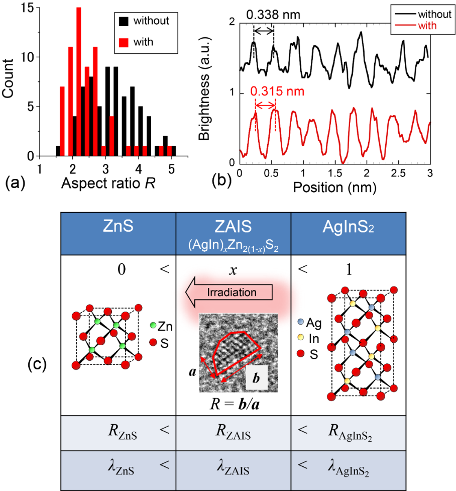
publisher = {Beilstein-Institut.},

abstract = {ZnS-AgInS2 (ZAIS) solid-solution nanocrystals are promising materials for nanophotonic devices in the visible region because of their low toxicity and good emission properties. We developed a technique of photo-induced synthesis to control the size and composition of the ZAIS nanocrystals. This method successfully decreased the defect levels, as well as the size and size variation of ZAIS nanocrystals by controlling the excitation wavelength during synthesis. Detailed analysis of transmission electron microscope images confirmed that the photo-induced synthesis yielded a high crystallinity of the ZAIS nanocrystals with small variations in size and content.},

keywords = {First, Nanophotonic fabrication, ZAIS},

pubstate = {published},

tppubtype = {article}

}
Hac Huong Thu Le, Kazuma Mawatari, Yuriy Pihosh, Tadashi Kawazoe, Takashi Yatsui, Motoichi Ohtsu, Takehiko Kitamori
Novel sub-100 nm surface chemical modification by optical near-field induced photocatalytic reaction Journal Article
In: Microfluidics and Nanofluidics, vol. 17, no. 4, pp. 751-758, 2014.
Abstract | Links | BibTeX | タグ: Nanophotonic fabrication, Near-field effect, Photocatalytic reaction
@article{2014Le,

title = {Novel sub-100 nm surface chemical modification by optical near-field induced photocatalytic reaction},

author = {Hac Huong Thu Le and Kazuma Mawatari and Yuriy Pihosh and Tadashi Kawazoe and Takashi Yatsui and Motoichi Ohtsu and Takehiko Kitamori},

doi = {10.1007/s10404-014-1361-7},

year  = {2014},

date = {2014-10-01},

journal = {Microfluidics and Nanofluidics},

volume = {17},

number = {4},

pages = {751-758},

publisher = {Springer Nature},

abstract = {The surface modification is indispensable to facilitate new functional applications of micro/nanofluidics devices. Among many modification techniques developed so far, the photo-induced chemical modification is the most versatile method in terms of robustness, process simplicity, and feasibility of chemical functionality. In particular, the method is useful for closed spaces, such as post-bonded devices. However, the limitation by optical diffraction limit is still a challenging issue in scaling down the pattern sizes to nanoscale. Here, we demonstrated a novel surface modification on sub-100 nm scale utilizing the novel optical near-field (ONF) generated on nanostructures of photocatalyst (TiO2). The minimum pattern size of 40 nm, which was much smaller than diffraction limit, was achieved using a visible light source (488 nm) and a conventional irradiation setup. The controllability of pattern size by light intensity, the feasibility of functionality, and the non-contact working mode have impacts on surface patterning of post-bonded micro/nanofluidics devices. It is also worthy to note that our results verified for the first time the ONF on nanostructures of non-metal materials and its ability to manipulate the chemical reaction on nanoscale.},

keywords = {Nanophotonic fabrication, Near-field effect, Photocatalytic reaction},

pubstate = {published},

tppubtype = {article}

}
Takashi Yatsui, Daisuke Takeuchi, Satoshi Koizumi, Kazuki Sato, Kohei Tsuzuki, Takayuki Iwasaki, Mutsuko Hatano, Toshiharu Makino, Masahiko Ogura, Hiromitsu Kato, Hideyo Okushi, Satoshi Yamasaki
Polarization-controlled dressed-photon–phonon etching of patterned diamond structures Journal Article
In: physica status solidi (a), vol. 211, no. 10, pp. 2339-2342, 2014.
Abstract | Links | BibTeX | タグ: Diamond, First, Nanophotonic fabrication, Near-field etching
@article{doi:10.1002/pssa.201431161,

title = {Polarization-controlled dressed-photon–phonon etching of patterned diamond structures},

author = {Takashi Yatsui and Daisuke Takeuchi and Satoshi Koizumi and Kazuki Sato and Kohei Tsuzuki and Takayuki Iwasaki and Mutsuko Hatano and Toshiharu Makino and Masahiko Ogura and Hiromitsu Kato and Hideyo Okushi and Satoshi Yamasaki},

doi = {10.1002/pssa.201431161},

year  = {2014},

date = {2014-10-01},

journal = {physica status solidi (a)},

volume = {211},

number = {10},

pages = {2339-2342},

abstract = {To realize an ultra-flat diamond surface with a three-dimensional (3D) structure, we performed dressed-photon–phonon (DPP) etching. A DPP is generated on nano-scale protrusions. Hence, the generation of DPPs results in selective removal of nano-scale protrusions, thereby achieving an ultra-flat surface even on the sidewall of a diamond mesa structure. By controlling the polarization of the incident light, a smooth diamond mesa structure sidewall was obtained, and a higher etching rate was obtained with a perpendicular polarization on the corrugations. In addition, by selective deposition of n-layer diamond on the p-layer diamond mesa structure, smooth n-layer diamond was confirmed on the DPP etched sidewall. Schematic of dressed-photon–phonon (DPP) etching on the sidewall: (a) before and (b) after etching, in which DPP selectively generates on the corrugations and etching automatically stops when the surface was smooth. Scanning electron microscopy image of the selective deposition of the n-layer (c) without and (d) with the DPP etched sidewall.},

keywords = {Diamond, First, Nanophotonic fabrication, Near-field etching},

pubstate = {published},

tppubtype = {article}

}
Pham Nam Hai, Takashi Yatsui, Motoichi Ohtsu, Masaaki Tanaka
High-field electroluminescence in semiconductor tunnel junctions with a Mn-doped GaAs layer Journal Article
In: Journal of Applied Physics, vol. 116, no. 11, pp. 113905, 2014.
Abstract | Links | BibTeX | タグ: EL, GaAs:Mn
@article{2014Hai,

title = {High-field electroluminescence in semiconductor tunnel junctions with a Mn-doped GaAs layer},

author = {Pham Nam Hai and Takashi Yatsui and Motoichi Ohtsu and Masaaki Tanaka},

doi = {10.1063/1.4895700},

year  = {2014},

date = {2014-09-01},

urldate = {2014-09-01},

journal = {Journal of Applied Physics},

volume = {116},

number = {11},

pages = {113905},

abstract = {We investigated high-field electroluminescence (EL) in semiconductor tunnel junctions with a Mn-doped GaAs layer (here, referred to as GaAs:Mn). Besides the band-gap emission of GaAs, the EL spectra show visible light emissions with two peaks at 1.94 eV and 2.19 eV, which are caused by d-d transitions of the Mn atoms excited by hot electrons. The threshold voltages for band-gap and visible light EL in the tunnel junctions with a GaAs:Mn electrode are 1.3 V higher than those of GaAs:Mn excited by hot holes in reserve biased p+-n junctions, which is consistent with the hot carrier transport in the band profiles of these structures. Our EL results at room temperature show that the electron temperature in GaAs:Mn can be as high as ∼700 K for a low input electrical power density of 0.4 W/cm2, while the lattice temperature of the GaAs:Mn layer can be kept at 340 K.

I. INTRODUCTION},

keywords = {EL, GaAs:Mn},

pubstate = {published},

tppubtype = {article}

}
I. INTRODUCTION
Wataru Nomura, Tadashi Kawazoe, Takashi Yatsui, Makoto Naruse, Motoichi Ohtsu
In: Beilstein Journal of Nanotechnology, vol. 5, pp. 1334-1340, 2014.
Abstract | Links | BibTeX | タグ: Nanophotonic fabrication, Near-field etching
@article{2014ZAISBJb,
title = {Observation and analysis of structural changes in fused silica by continuous irradiation with femtosecond laser light having an energy density below the laser-induced damage threshold},
author = {Wataru Nomura and Tadashi Kawazoe and Takashi Yatsui and Makoto Naruse and Motoichi Ohtsu},
doi = {10.3762/bjnano.5.146},
year = {2014},
date = {2014-08-01},
journal = {Beilstein Journal of Nanotechnology},
volume = {5},
pages = {1334-1340},
publisher = {Beilstein-Institut.},
abstract = {The laser-induced damage threshold (LIDT) is widely used as an index for evaluating an optical componentfs resistance to laser light. However, a degradation in the performance of an optical component is also caused by continuous irradiation with laser light having an energy density below the LIDT. Therefore, here we focused on the degradation in performance of an optical component caused by continuous irradiation with femtosecond laser light having a low energy density, i.e., laser-induced degradation. We performed an in situ observation and analysis of an increase in scattering light intensity in fused silica substrates. In experiments conducted using a pulsed laser with a wavelength of 800 nm, a pulse width of 160 fs and pulse repetition rate of 1 kHz, we found that the scattered light intensity increased starting from a specific accumulated fluence, namely, that the laser-induced degradation had a threshold. We evaluated the threshold fluence Ft as 6.27 J/cm2 and 9.21 J/cm2 for the fused silica substrates with surface roughnesses of 0.20 nm and 0.13 nm in Ra value, respectively, showing that the threshold decreased as the surface roughness increased. In addition, we found that the reflected light spectrum changed as degradation proceeded. We analyzed the details of the degradation by measuring instantaneous reflectance changes with a pump-probe method; we observed an increase in the generation probability of photogenerated carriers in a degraded silica substrate and a damaged silica substrate and observed a Raman signal originating from a specific molecular structure of silica. From these findings, we concluded that compositional changes in the molecular structure occurred during degradation due to femtosecond laser irradiation having an energy density below the LIDT.},
keywords = {Nanophotonic fabrication, Near-field etching},
pubstate = {published},
tppubtype = {article}
}
Hiroaki Matsui, Wasanthamala Badalawa, Takayuki Hasebe, Shinya Furuta, Wataru Nomura, Takashi Yatsui, Motoichi Ohtsu, Hitoshi Tabata
Coupling of Er light emissions to plasmon modes on In2O3: Sn nanoparticle sheets in the near-infrared range Journal Article
In: Applied Physics Letters, vol. 105, no. 4, pp. 041903, 2014.
Abstract | Links | BibTeX | タグ: In2O3: Sn, Plasmon, ZnO
@article{2014Matsui,

title = {Coupling of Er light emissions to plasmon modes on In2O3: Sn nanoparticle sheets in the near-infrared range},

author = {Hiroaki Matsui and Wasanthamala Badalawa and Takayuki Hasebe and Shinya Furuta and Wataru Nomura and Takashi Yatsui and Motoichi Ohtsu and Hitoshi Tabata},

doi = {10.1063/1.4892004},

year  = {2014},

date = {2014-07-01},

urldate = {2014-07-01},

journal = {Applied Physics Letters},

volume = {105},

number = {4},

pages = {041903},

abstract = {Near-infrared Er photoluminescence (PL) is markedly modified using a plasmonic In2O3: Sn nanoparticle (NP) sheet. Modeling and optical measurements reveal the presence of different electric fields (E-field) in the NP sheet. The local E-field excited at the interface between the NP sheet and Er-emitting layer of ZnO contributes significantly towards the spectral modifications of Er PL due to matching with the photon energy of Er PL. We also determine the critical temperature for Er PL modifications, which is related to the energy transfer efficiency between Er transition dipoles in ZnO and the plasmon modes on the NP sheet.},

keywords = {In2O3: Sn, Plasmon, ZnO},

pubstate = {published},

tppubtype = {article}

}
Takashi Yatsui, Tsubasa Imoto, Takahiro Mochizuki, Kokoro Kitamura, Tadashi Kawazoe
Dressed-photon–phonon (DPP)-assisted visible- and infrared-light water splitting Journal Article
In: Scientific Reports, vol. 4, pp. 4561, 2014.
Abstract | Links | BibTeX | タグ: First, Non-uniform optical near field, Water splitting, ZnO
@article{2014water,

title = {Dressed-photon–phonon (DPP)-assisted visible- and infrared-light water splitting},

author = {Takashi Yatsui and Tsubasa Imoto and Takahiro Mochizuki and Kokoro Kitamura and Tadashi Kawazoe},

doi = {10.1038/srep04561},

year  = {2014},

date = {2014-04-01},

journal = {Scientific Reports},

volume = {4},

pages = {4561},

publisher = {Springer Nature},

abstract = {A dressed-phonon–phonon (DPP) assisted photocatalyst reaction was carried out to increase the visible light responsibility, where the photon energy of the radiation, which ranged from visible to infrared light is less than band gap energy of the photocatalyst (ZnO, 3.3 eV). The dependence of the photocurrent on excitation power indicated that two-step excitation occurred in DPP-assisted process. A cathodoluminescence measurement also supported the conclusion that the visible- and infrared-light excitation originated from DPP excitation, not from defect states in the ZnO nanorod photocatalyst.},

keywords = {First, Non-uniform optical near field, Water splitting, ZnO},

pubstate = {published},

tppubtype = {article}

}
Takashi Yatsui, Wataru Nomura, Takaaki Mano, Hideki Miyazaki, Kazuaki Sakoda, Tadashi Kawazoe, Motoichi Ohtsu
Emission from a dipole-forbidden energy state in a GaAs quantum-ring induced by dressed photon Journal Article
In: Applied Physics A, vol. 115, no. 1, pp. 1-4, 2014.
Abstract | Links | BibTeX | タグ: First, GaAs, Non-uniform optical near field, Quantum-ring
@article{2014YatsuiGaAsAPA,

title = {Emission from a dipole-forbidden energy state in a GaAs quantum-ring induced by dressed photon},

author = {Takashi Yatsui and Wataru Nomura and Takaaki Mano and Hideki Miyazaki and Kazuaki Sakoda and Tadashi Kawazoe and Motoichi Ohtsu},

doi = {10.1007/s00339-013-7905-y},

year  = {2014},

date = {2014-04-01},

urldate = {2014-04-01},

journal = {Applied Physics A},

volume = {115},

number = {1},

pages = {1-4},

publisher = {Springer Nature},

abstract = {The emission intensity from the dipole-forbidden state in a GaAs quantum-ring was increased via close proximity with an aperture fiber probe to induce a near-field interaction between the probe apex and the quantum-ring. As a result, a significant decrease was observed in the decay time of the emission from a dipole-forbidden energy state.},

keywords = {First, GaAs, Non-uniform optical near field, Quantum-ring},

pubstate = {published},

tppubtype = {article}

}
Wataru Nomura, Makoto Naruse, Masashi Aono, Song-Ju Kim, Tadashi Kawazoe, Takashi Yatsui, Motoichi Ohtsu
In: Advances in Optical Technologies, vol. 2014, pp. 569684, 2014.
Abstract | Links | BibTeX | タグ: Nanophotonic device, Near-field effect, QD
@article{2014NomuraY,

title = {Demonstration of Controlling the Spatiotemporal Dynamics of Optical Near-Field Excitation Transfer in Y-Junction Structure Consisting of Randomly Distributed Quantum Dots},

author = {Wataru Nomura and Makoto Naruse and Masashi Aono and Song-Ju Kim and Tadashi Kawazoe and Takashi Yatsui and Motoichi Ohtsu},

doi = {10.1155/2014/569684},

year  = {2014},

date = {2014-02-01},

urldate = {2014-02-01},

journal = {Advances in Optical Technologies},

volume = {2014},

pages = {569684},

abstract = {Solution searching devices that operate on the basis of controlling the spatiotemporal dynamics of excitation transfer via dressed photon interactions between quantum dots have been proposed. Long-range excitation transfer based on dressed photon interactions between randomly distributed quantum dots is considered to be effective in realizing such devices. Here, we successfully controlled the spatiotemporal dynamics of excitation transfer using a Y-junction structure consisting of randomly dispersed CdSe/ZnS core-shell quantum dots. This Y-junction structure has two “output ends” and one “tap end.” By exciting one output end with control light, we observed increased excitation transfer to the other output end via a state-filling effect. Conversely, we observed reduced excitation transfer to the output ends by irradiating the tap end with control light, due to excitation of defect levels in the tap end. These results show the possibility of controlling the optical excitation transfer dynamics between multiple quantum dots.},

keywords = {Nanophotonic device, Near-field effect, QD},

pubstate = {published},

tppubtype = {article}

}
2013
Takashi Yatsui, Wataru Nomura, Fabrice Stehlin, Olivier Soppera, Makoto Naruse, Motoichi Ohtsu
Challenge in realizing ultraflat material surfaces Journal Article
In: Beilstein Journal of Nanotechnology, vol. 4, pp. 875-885, 2013, (review article).
Abstract | Links | BibTeX | タグ: First, Nanophotonic fabrication, Near-field etching, Review, Selected
@article{2013yatsuiBJrev,
title = {Challenge in realizing ultraflat material surfaces},
author = {Takashi Yatsui and Wataru Nomura and Fabrice Stehlin and Olivier Soppera and Makoto Naruse and Motoichi Ohtsu},
doi = {10.3762/bjnano.4.99},
year = {2013},
date = {2013-12-01},
journal = {Beilstein Journal of Nanotechnology},
volume = {4},
pages = {875-885},
publisher = {Beilstein-Institut.},
abstract = {The laser-induced damage threshold (LIDT) is widely used as an index for evaluating an optical componentfs resistance to laser light. However, a degradation in the performance of an optical component is also caused by continuous irradiation with laser light having an energy density below the LIDT. Therefore, here we focused on the degradation in performance of an optical component caused by continuous irradiation with femtosecond laser light having a low energy density, i.e.Ultraflat surface substrates are required to achieve an optimal performance of future optical, electronic, or optoelectronic devices for various applications, because such surfaces reduce the scattering loss of photons, electrons, or both at the surfaces and interfaces. In this paper, we review recent progress toward the realization of ultraflat materials surfaces. First, we review the development of surface-flattening techniques. Second, we briefly review the dressed photon-phonon (DPP), a nanometric quasiparticle that describes the coupled state of a photon, an electron, and a multimode-coherent phonon. Then, we review several recent developments based on DPP-photochemical etching and desorption processes, which have resulted in angstrom-scale flat surfaces. To confirm that the superior flatness of these surfaces that originated from the DPP process, we also review a simplified mathematical model that describes the scale-dependent effects of optical near-fields. Finally, we present the future outlook for these technologies.},
note = {review article},
keywords = {First, Nanophotonic fabrication, Near-field etching, Review, Selected},
pubstate = {published},
tppubtype = {article}
}
Nabila Tanjeem, Tadashi Kawazoe, Takashi Yatsui
CO2 phonon mode renormalization using phonon-assisted energy up-conversion Journal Article
In: Scientific Reports, vol. 3, pp. 3341, 2013.
Abstract | Links | BibTeX | タグ: CO2 reduction, Non-uniform optical near field
@article{2013nabilaSR,

title = {CO2 phonon mode renormalization using phonon-assisted energy up-conversion},

author = {Nabila Tanjeem and Tadashi Kawazoe and Takashi Yatsui},

doi = {10.1038/srep03341},

year  = {2013},

date = {2013-11-01},

journal = {Scientific Reports},

volume = {3},

pages = {3341},

publisher = {Springer Nature},

abstract = {Molecular dissociation under incident light whose energy is lower than the bond dissociation energy has been achieved through multi step excitation using a coupled state of a photon, electron and multimode-coherent phonon as known as the dressed photon phonon (DPP). Here, we have investigated the effects of the DPP on CO2, a very stable molecule with high absorption and dissociation energies, by introducing ZnO nanorods to generate the DPP. Then, the changes in CO2 absorption bands were evaluated using light with a wavelength longer than the absorption wavelength, which confirmed the DPP-assisted energy up-conversion. To evaluate the specific CO2 modes related to this process, we measured the CO2 vibration-rotation spectra in the near-infrared region. Detailed analysis of the 3ν3 vibrational band when a DPP source is present showed that DPP causes a significant increase in the intensity of certain absorption bands, especially those that require higher energies to activate.},

keywords = {CO2 reduction, Non-uniform optical near field},

pubstate = {published},

tppubtype = {article}

}
