Publications
ResearcherID : C-5956-2008 (TY, h-index: 25) , AAZ-8749-2021 (RK, h-index: 13)
Google Scholar : TY (h-index: 35), RK (h-index: 14), KT (h-index: 4)
Research Square: TY
2025
Kosuke Takada, Ryota Katsumi, Daichi Sato, Kenta Kawai, Takashi Yatsui
High-Q plasmonic resonances from a transfer-printed diamond ring on a silver surface Journal Article
In: Japanese Journal of Applied Physics, vol. 64, iss. 8, pp. 080903, 2025.
Abstract | Links | BibTeX | タグ: Diamond, nanophotonics, Plasmon
@article{plasmonicring,
title = {High-Q plasmonic resonances from a transfer-printed diamond ring on a silver surface},
author = {Kosuke Takada and Ryota Katsumi and Daichi Sato and Kenta Kawai and Takashi Yatsui},
doi = {10.35848/1347-4065/adf618},
year = {2025},
date = {2025-08-14},
journal = {Japanese Journal of Applied Physics},
volume = {64},
issue = {8},
pages = {080903},
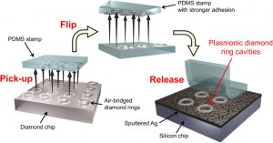
abstract = {Optically addressable point defects in diamond are promising physical platforms in quantum technologies. In particular, defects embedded in plasmonic devices can interact strongly with photons and provide a robust approach to engineering spin-photon interfaces. However, diamond-based plasmonic devices have low quality factors of Q<10, constrained by fabrication difficulties. This study demonstrates the high-Q plasmonic resonance of optical emissions from nitrogen-vacancy centers in diamond ring structures onto a silver surface, and experimentally shows that Q~179. The proposed device can be easily fabricated using the transfer printing technique. These results address the lack of high-Q plasmonic cavities in diamond-based technologies.},
keywords = {Diamond, nanophotonics, Plasmon},
pubstate = {published},
tppubtype = {article}
}
Kosuke Takada, Ryota Katsumi, Kenta Kawai, Daichi Sato, Takashi Yatsui
Alignment-tolerant hybrid integration of a diamond quantum sensor on a silicon nitride photonic waveguide Journal Article
In: Optics Express, vol. 33, iss. 11, pp. 22769-22779, 2025.
Abstract | Links | BibTeX | タグ: Diamond, nanophotonics
@article{alignmentfree,
title = {Alignment-tolerant hybrid integration of a diamond quantum sensor on a silicon nitride photonic waveguide},
author = {Kosuke Takada and Ryota Katsumi and Kenta Kawai and Daichi Sato and Takashi Yatsui},
doi = {10.1364/OE.559486},
year = {2025},
date = {2025-05-24},
urldate = {2025-05-24},
journal = {Optics Express},
volume = {33},
issue = {11},
pages = {22769-22779},
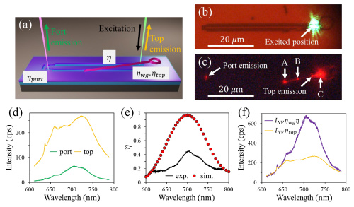
abstract = {Hybrid-integrated photonic circuits play a crucial role in recent quantum technologies. However, deterministic and alignment-tolerant methods are still lacking, and their development is crucial for accelerating the scalable fabrication of quantum systems. In this study, we demonstrate alignment-tolerant coupling between diamond and silicon nitride waveguides using the deterministic transfer-printing method. To validate this approach, we also demonstrate the capability of on-chip quantum sensing using nitrogen vacancy centers in diamond waveguides. These results pave the way for compact packaging of highly sensitive quantum sensors based on photonic integrated circuits.},
keywords = {Diamond, nanophotonics},
pubstate = {published},
tppubtype = {article}
}