Publications
ResearcherID : C-5956-2008 (TY, h-index: 25) , AAZ-8749-2021 (RK, h-index: 13)
Google Scholar : TY (h-index: 35), RK (h-index: 14), KT (h-index: 4)
Research Square: TY
2021

Zhiyu Wang, Ya‐Lun Ho, Tun Cao, Takashi Yatsui, Jean‐Jacques Delaunay
In: Advanced Functional Materials, 2021.
Abstract | Links | BibTeX | タグ: Selected, Tamm state
@article{advfunmat21,

title = {High‐Q and Tailorable Fano Resonances in a One‐Dimensional Metal‐Optical Tamm State Structure: From a Narrowband Perfect Absorber to a Narrowband Perfect Reflector},

author = {Zhiyu Wang and Ya‐Lun Ho and Tun Cao and Takashi Yatsui and Jean‐Jacques Delaunay},

doi = {10.1002/adfm.202102183},

year  = {2021},

date = {2021-04-19},

urldate = {2021-04-19},

journal = {Advanced Functional Materials},

abstract = {Fano resonances giving rise to a rich variety of asymmetric spectral shapes have been investigated in optical nanostructures with multidimensional configurations. However, 1D nanostructure realizing Fano resonances with well‐controlled spectral shapes are yet to be demonstrated. Here, the authors present both numerically and experimentally a 1D nanostructure exhibiting rich Fano resonances induced by interference between a lossy background (continuum) provided by a metal thin film and a discrete optical Tamm state (OTS). A drastic change in the Fano line shape occurs from a narrowband perfect absorber into a narrowband perfect reflector by controlling the metal thin film. Independent from the metal‐related Fano profile, the OTS component determines the resonance frequency and guarantees a sharp resonance (with quality factors over 1000) on the flat mirror background. Taking advantage of its high‐Q property, the structure can be developed into a dispersion device with subnanometer spectral resolution, which even enables a direct imaging of spectral information of molecular fingerprint. The authors believe that this work not only demonstrates a planar nanostructure with versatile Fano resonances for various applications but also provides physical insights into how a metal thin film can induce and significantly affect the Fano resonances in 1D optical resonators.},

keywords = {Selected, Tamm state},

pubstate = {published},

tppubtype = {article}

}
2019
Takashi Yatsui, Syunsuke Okada, Tatsuya Takemori, Takumi Sato, Kota Saichi, Tatsuro Ogamoto, Shohei Chiashi, Shigeo Maruyama, Masashi Noda, Kazuhiro Yabana, Kenji Iida, Katsuyuki Nobusada
Enhanced photo-sensitivity in a Si photodetector using a near-field assisted excitation Journal Article
In: Communications Physics, vol. 2, pp. 62, 2019.
Abstract | Links | BibTeX | タグ: Direct wave-vector excitation, First, Selected, Si photodetector
@article{yatsui2019Si,
title = {Enhanced photo-sensitivity in a Si photodetector using a near-field assisted excitation},
author = {Takashi Yatsui and Syunsuke Okada and Tatsuya Takemori and Takumi Sato and Kota Saichi and Tatsuro Ogamoto and Shohei Chiashi and Shigeo Maruyama and Masashi Noda and Kazuhiro Yabana and Kenji Iida and Katsuyuki Nobusada},
doi = {10.1038/s42005-019-0173-1},
year = {2019},
date = {2019-06-01},
journal = {Communications Physics},
volume = {2},
pages = {62},
publisher = {Springer Nature},
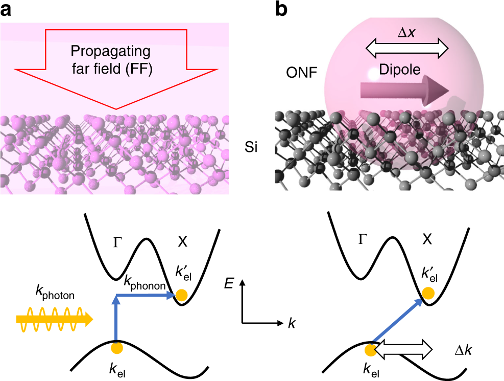
abstract = {Silicon is an indispensable material in electric device technology. However, Si is an indirect bandgap material; therefore, its excitation efficiency, which requires phonon assistance, is low under propagating far-field light. To improve the excitation efficiency, herein we performed optical near-field excitation, which is confined in a nano-scale, where the interband transitions between different wave numbers are excited according to the uncertainty principle; thus, optical near-field can directly excite the carrier in the indirect bandgap. To evaluate the effect of optical near-field confined in a nano-scale, we fabricate the lateral Si p-n junction with Au nanoparticles as sources to generate the field confinement. We observed a 47.0 % increase in the photo-sensitivity rate. In addition, by using the thin lateral p-n junction, which eliminates the far-field excitation, we confirmed a 42.3 % increase in the photo-sensitivity rate.},
keywords = {Direct wave-vector excitation, First, Selected, Si photodetector},
pubstate = {published},
tppubtype = {article}
}
2017

Takashi Yatsui, Maiku Yamaguchi, Katsuyuki Nobusada
Nano-scale chemical reactions based on non-uniform optical near-fields and their applications Journal Article
In: Progress in Quantum Electronics, vol. 55, pp. 166 - 194, 2017, ISSN: 0079-6727, (review article).
Abstract | Links | BibTeX | タグ: Artificial photosynthesis, First, Near-field etching, Non-uniform optical near field, Photodissociation path with two-step excitation, Review, Selected, SHG
@article{YATSUI2017166,

title = {Nano-scale chemical reactions based on non-uniform optical near-fields and their applications},

author = {Takashi Yatsui and Maiku Yamaguchi and Katsuyuki Nobusada},

doi = {10.1016/j.pquantelec.2017.06.001},

issn = {0079-6727},

year  = {2017},

date = {2017-09-01},

journal = {Progress in Quantum Electronics},

volume = {55},

pages = {166 - 194},

abstract = {Interaction between light and materials is essential in the physics underlying all optical devices, including light emitting devices such as light emitting diodes and lasers, photo-voltaic devices, and photo-synthesis systems. The demand for higher light utilization efficiency is becoming increasingly important for advanced optical devices. This is because, when feature size is smaller than the incident light wavelength, photons cannot couple with devices efficiently. In this paper, we review recent progress regarding a unique phenomenon at the nano scale and its applications. First, we summarize the development of light–matter interactions at the nano-scale. Second, we review recent theoretical works focusing on optical near fields in which unique phenomena arise from non-uniform optical fields. We then review several recent developments based on the near-field effect, including artificial photosynthesis and near-field etching for realization of angstrom-scale fattened surfaces. Finally, we discuss the future outlook for these technologies.},

note = {review article},

keywords = {Artificial photosynthesis, First, Near-field etching, Non-uniform optical near field, Photodissociation path with two-step excitation, Review, Selected, SHG},

pubstate = {published},

tppubtype = {article}

}
2016
Takashi Yatsui, Toshiki Tsuboi, Maiku Yamaguchi, Katsuyuki Nobusada, Satoshi Tojo, Fabrice Stehlin, Olivier Soppera, Daniel Bloch
Optically controlled magnetic-field etching on the nano-scale Journal Article
In: Light: Science & Applications, vol. 5, pp. e16054, 2016.
Abstract | Links | BibTeX | タグ: First, Nanophotonic fabrication, Near-field etching, Selected
@article{2016YatsuiLST,

title = {Optically controlled magnetic-field etching on the nano-scale},

author = {Takashi Yatsui and Toshiki Tsuboi and Maiku Yamaguchi and Katsuyuki Nobusada and Satoshi Tojo and Fabrice Stehlin and Olivier Soppera and Daniel Bloch},

url = {https://www.altmetric.com/details/6399772},

doi = {10.1038/lsa.2016.54},

year  = {2016},

date = {2016-03-25},

journal = {Light: Science & Applications},

volume = {5},

pages = {e16054},

publisher = {Springer Nature},

abstract = {Electric and magnetic fields play an important role in both chemical and physical reactions. However, since the coupling efficiency between magnetic fields and electrons is low in comparison with that between electric fields and electrons in the visible wavelength region, the magnetic field is negligible in photo-induced reactions. Here, we performed photo-etching of ZrO2 nano-stripe structures, and identified an etching-property polarisation dependence. Specifically, the etching rate and etched profiles depend on the structure width. To evaluate this polarisation-dependent etching, we performed numerical calculations using a finite-difference time-domain method. Remarkably, the numerical results revealed that the polarisation-dependent etching properties were determined by the magnetic field distributions, rather than the electric field distributions. As nano-scale structures induce a localised magnetic field, the discovery of this etching dependence on the magnetic field is expected to introduce a new perspective on advanced nano-scale structure fabrication.},

keywords = {First, Nanophotonic fabrication, Near-field etching, Selected},

pubstate = {published},

tppubtype = {article}

}
2015
Maiku Yamaguchi, Katsuyuki Nobusada, Takashi Yatsui
Nonlinear optical response induced by a second-harmonic electric-field component concomitant with optical near-field excitation Journal Article
In: Phys. Rev. A, vol. 92, no. 4, pp. 043809, 2015.
Abstract | Links | BibTeX | タグ: Non-uniform optical near field, Selected, SHG
@article{PhysRevA.92.043809,

title = {Nonlinear optical response induced by a second-harmonic electric-field component concomitant with optical near-field excitation},

author = {Maiku Yamaguchi and Katsuyuki Nobusada and Takashi Yatsui},

doi = {10.1103/PhysRevA.92.043809},

year  = {2015},

date = {2015-10-01},

journal = {Phys. Rev. A},

volume = {92},

number = {4},

pages = {043809},

publisher = {American Physical Society},

abstract = {Electron dynamics excited by an optical near field (ONF) in a two-dimensional quantum dot model was investigated by solving a time-dependent Schrödinger equation. It was found that the ONF excitation of the electron caused two characteristic phenomena: a two-photon absorption and an induction of a magnetic dipole moment with a strong third-harmonic component. By analyzing the interaction dynamics of the ONF and the electron, we explained that the physical mechanism underlying these phenomena was the second-harmonic electric-field component concomitant with the near-field excitation originating from the nonuniformity of the ONF. Despite a y-polarized ONF source, the second-harmonic component of an

x-polarized electric field was inherently generated. The effect of the second-harmonic electric-field component is not due to usual second-order nonlinear response but appears only when we explicitly consider the electron dynamics interacting with the ONF beyond the conventional optical response assuming the dipole approximation.},

keywords = {Non-uniform optical near field, Selected, SHG},

pubstate = {published},

tppubtype = {article}

}
x-polarized electric field was inherently generated. The effect of the second-harmonic electric-field component is not due to usual second-order nonlinear response but appears only when we explicitly consider the electron dynamics interacting with the ONF beyond the conventional optical response assuming the dipole approximation.
2013

Takashi Yatsui, Wataru Nomura, Fabrice Stehlin, Olivier Soppera, Makoto Naruse, Motoichi Ohtsu
Challenge in realizing ultraflat material surfaces Journal Article
In: Beilstein Journal of Nanotechnology, vol. 4, pp. 875-885, 2013, (review article).
Abstract | Links | BibTeX | タグ: First, Nanophotonic fabrication, Near-field etching, Review, Selected
@article{2013yatsuiBJrev,
title = {Challenge in realizing ultraflat material surfaces},
author = {Takashi Yatsui and Wataru Nomura and Fabrice Stehlin and Olivier Soppera and Makoto Naruse and Motoichi Ohtsu},
doi = {10.3762/bjnano.4.99},
year = {2013},
date = {2013-12-01},
journal = {Beilstein Journal of Nanotechnology},
volume = {4},
pages = {875-885},
publisher = {Beilstein-Institut.},
abstract = {The laser-induced damage threshold (LIDT) is widely used as an index for evaluating an optical componentfs resistance to laser light. However, a degradation in the performance of an optical component is also caused by continuous irradiation with laser light having an energy density below the LIDT. Therefore, here we focused on the degradation in performance of an optical component caused by continuous irradiation with femtosecond laser light having a low energy density, i.e.Ultraflat surface substrates are required to achieve an optimal performance of future optical, electronic, or optoelectronic devices for various applications, because such surfaces reduce the scattering loss of photons, electrons, or both at the surfaces and interfaces. In this paper, we review recent progress toward the realization of ultraflat materials surfaces. First, we review the development of surface-flattening techniques. Second, we briefly review the dressed photon-phonon (DPP), a nanometric quasiparticle that describes the coupled state of a photon, an electron, and a multimode-coherent phonon. Then, we review several recent developments based on DPP-photochemical etching and desorption processes, which have resulted in angstrom-scale flat surfaces. To confirm that the superior flatness of these surfaces that originated from the DPP process, we also review a simplified mathematical model that describes the scale-dependent effects of optical near-fields. Finally, we present the future outlook for these technologies.},
note = {review article},
keywords = {First, Nanophotonic fabrication, Near-field etching, Review, Selected},
pubstate = {published},
tppubtype = {article}
}
2012
Manfred Mascheck, Stephen Schmidt, Martin Silies, Takashi Yatsui, Kokoro Kitamura, Motoichi Ohtsu, David Leipold, Erich Runge, Christoph Lienau
Observing the localization of light in space and time by ultrafast second-harmonic microscopy Journal Article
In: Nature Photonics, vol. 6, no. 5, pp. 293-298, 2012.
Abstract | Links | BibTeX | タグ: Near-field effect, Selected, SHG
@article{2012NatPhoton,

title = {Observing the localization of light in space and time by ultrafast second-harmonic microscopy},

author = {Manfred Mascheck and Stephen Schmidt and Martin Silies and Takashi Yatsui and Kokoro Kitamura and Motoichi Ohtsu and David Leipold and Erich Runge and Christoph Lienau},

url = {https://www.altmetric.com/details/698801},

doi = {10.1038/nphoton.2012.69},

year  = {2012},

date = {2012-05-01},

journal = {Nature Photonics},

volume = {6},

number = {5},

pages = {293-298},

publisher = {Springer Nature},

abstract = {Multiple coherent scattering and the constructive interference of certain scattering paths form the common scheme of several remarkable localization phenomena of classical and quantum waves in randomly disordered media. Prominent examples are electron transport in disordered conductors, the localization of excitons in semiconductor nanostructures, surface plasmon polaritons at rough metallic films or light in disordered dielectrics and amplifying media. However, direct observation of the fundamental spatiotemporal dynamics of the localization process remains challenging. This holds true, in particular, for the localization of light occurring on exceedingly short femtosecond timescales and nanometre length scales. Here, we combine second harmonic microscopy with few-cycle time resolution to probe the spatiotemporal localization of light waves in a random dielectric medium. We find lifetimes of the photon modes of several femtoseconds and a broad distribution of the local optical density of states, revealing central hallmarks of the localization of light.},

keywords = {Near-field effect, Selected, SHG},

pubstate = {published},

tppubtype = {article}

}
2008
Takashi Yatsui, Kazuya Hirata, Wataru Nomura, Yoshinori Tabata, Motoichi Ohtsu
Realization of an ultra-flat silica surface with angstrom-scale average roughness using nonadiabatic optical near-field etching Journal Article
In: Applied Physics B, vol. 93, no. 1, pp. 55-57, 2008.
Abstract | Links | BibTeX | タグ: First, Nanophotonic fabrication, Near-field etching, Selected
@article{2008yatsuiAPBNFE,

title = {Realization of an ultra-flat silica surface with angstrom-scale average roughness using nonadiabatic optical near-field etching},

author = {Takashi Yatsui and Kazuya Hirata and Wataru Nomura and Yoshinori Tabata and Motoichi Ohtsu},

doi = {10.1007/s00340-008-3142-z},

year  = {2008},

date = {2008-10-01},

journal = {Applied Physics B},

volume = {93},

number = {1},

pages = {55-57},

publisher = {Springer Nature},

abstract = {We propose a new method of optical near-field etching where a nonadiabatic process is applied to a synthetic silica substrate using a continuum wave laser (λ=532 nm) with a Cl2 gas source. Because the absorption band edge energy of Cl2 is higher than the photon energy of the light source, we preclude the conventional adiabatic photochemical reaction. An optical near field, generated on the nanometrically rough substrate, induces the nonadiabatic chemical reaction to the Cl2 molecules and thereby selectively etches away the roughness, leaving an ultra-flat synthetic silica surface with a minimum average surface roughness R a of 1.37 A.},

keywords = {First, Nanophotonic fabrication, Near-field etching, Selected},

pubstate = {published},

tppubtype = {article}

}
2007

Takashi Yatsui, Suguru Sangu, Tadashi Kawazoe, Motoichi Ohtsu, Sung Jin An, Jinkyoung Yoo, Gyu-Chul Yi
Nanophotonic switch using ZnO nanorod double-quantum-well structures Journal Article
In: Applied Physics Letters, vol. 90, no. 22, pp. 223110, 2007.
Abstract | Links | BibTeX | タグ: First, Nanophotonic device, Selected, ZnO
@article{doi:10.1063/1.2743949,

title = {Nanophotonic switch using ZnO nanorod double-quantum-well structures},

author = {Takashi Yatsui and Suguru Sangu and Tadashi Kawazoe and Motoichi Ohtsu and Sung Jin An and Jinkyoung Yoo and Gyu-Chul Yi},

doi = {10.1063/1.2743949},

year  = {2007},

date = {2007-01-01},

urldate = {2007-01-01},

journal = {Applied Physics Letters},

volume = {90},

number = {22},

pages = {223110},

abstract = {The authors report on time-resolved near-field spectroscopy of ZnO∕ZnMgO nanorod double-quantum-well structures (DQWs) for a nanometer-scale photonic device. They observed nutation of the population between the resonantly coupled exciton states of DQWs. Furthermore, they demonstrated switching dynamics by controlling the exciton excitation in the dipole-inactive state via an optical near field. The results of time-resolved near-field spectroscopy of isolated DQWs described here are a promising step toward designing a nanometer-scale photonic switch and related devices.},

keywords = {First, Nanophotonic device, Selected, ZnO},

pubstate = {published},

tppubtype = {article}

}
2005

Takashi Yatsui, Wataru Nomura, Motoichi Ohtsu
Self-Assembly of Size- and Position-Controlled Ultralong Nanodot Chains using Near-Field Optical Desorption Journal Article
In: Nano Letters, vol. 5, no. 12, pp. 2548-2551, 2005, (PMID: 16351213).
Abstract | Links | BibTeX | タグ: First, Nanophotonic fabrication, Plasmon, Selected, Self-assembly
@article{doi:10.1021/nl051898z,

title = {Self-Assembly of Size- and Position-Controlled Ultralong Nanodot Chains using Near-Field Optical Desorption},

author = {Takashi Yatsui and Wataru Nomura and Motoichi Ohtsu},

doi = {10.1021/nl051898z},

year  = {2005},

date = {2005-12-01},

journal = {Nano Letters},

volume = {5},

number = {12},

pages = {2548-2551},

abstract = {We report the self-assembly of a size- and position-controlled ultralong nanodot chain using a novel effect of near-field optical desorption. A sub-100-nm dot chain with a deviation of 5 nm forms at a size based on plasmon resonance, depending on the photon energy; the resulting structure forms a high-transmission-efficiency nanoscale waveguide. Using this method with simple lithographically patterned substrates allows one to increase the throughput of the production of nanoscale structures dramatically at all scales.},

note = {PMID: 16351213},

keywords = {First, Nanophotonic fabrication, Plasmon, Selected, Self-assembly},

pubstate = {published},

tppubtype = {article}

}

Wataru Nomura, Motoichi Ohtsu, Takashi Yatsui
Nanodot coupler with a surface plasmon polariton condenser for optical far/near-field conversion Journal Article
In: Applied Physics Letters, vol. 86, no. 18, pp. 181108, 2005.
Abstract | Links | BibTeX | タグ: Plasmon, Selected
@article{doi:10.1063/1.1920419,

title = {Nanodot coupler with a surface plasmon polariton condenser for optical far/near-field conversion},

author = {Wataru Nomura and Motoichi Ohtsu and Takashi Yatsui},

doi = {10.1063/1.1920419},

year  = {2005},

date = {2005-05-01},

urldate = {2005-05-01},

journal = {Applied Physics Letters},

volume = {86},

number = {18},

pages = {181108},

abstract = {To transmit an optical signal to a nanophotonic device, a nanodot coupler was fabricated from a linear array of closely spaced metallic nanoparticles. To increase the optical far- to near-field conversion efficiency for transmission, a surface plasmon polariton (SPP) condenser was also fabricated from hemispherical metallic nanoparticles so that it worked as a “phased array”. The SPP was focused with a spot size as small as 400 nm at λ=785nm. When the focused SPP was incident into the nanodot coupler, its transmission length through the nanodot coupler was confirmed to be 4.0 μm, which is three times longer than that of a metallic core waveguide owing to the efficient near-field coupling between the localized surface plasmon of neighboring nanoparticles. Furthermore, the transmission length through a zigzag-shaped nanodot coupler was as long as that through a linear one.},

keywords = {Plasmon, Selected},

pubstate = {published},

tppubtype = {article}

}
2002
Motoichi Ohtsu, Kiyoshi Kobayashi, Tadashi Kawazoe, Suguru Sangu, Takashi Yatsui
Nanophotonics: design, fabrication, and operation of nanometric devices using optical near fields Journal Article
In: IEEE Journal of Selected Topics in Quantum Electronics, vol. 8, no. 4, pp. 839-862, 2002, (review article).
Abstract | Links | BibTeX | タグ: Nanophotonic device, Nanophotonic fabrication, Review, Selected
@article{2008IEEEb,

title = {Nanophotonics: design, fabrication, and operation of nanometric devices using optical near fields},

author = {Motoichi Ohtsu and Kiyoshi Kobayashi and Tadashi Kawazoe and Suguru Sangu and Takashi Yatsui},

doi = {10.1109/JSTQE.2002.801738},

year  = {2002},

date = {2002-07-01},

journal = {IEEE Journal of Selected Topics in Quantum Electronics},

volume = {8},

number = {4},

pages = {839-862},

publisher = {IEEE},

abstract = {This paper reviews progress in nanophotonics, a novel optical nanotechnology, utilizing local electromagnetic interactions between a few nanometric elements and an optical near field. A prototype of a nanophotonic integrated circuit (IC) is presented, in which the optical near field is used as a carrier to transmit a signal from one nanometric dot to another. Each section of this paper reviews theoretical and experimental studies carried out to assess the possibility of designing, fabricating, and operating each nanophotonic IC device. A key device, the nanophotonic switch, is proposed based on optical near-field energy transfer between quantum dots (QDs). The optical near-field interaction is expressed as the sum of the Yukawa function, and the oscillation period of the nutation of cubic CuCl QDs is estimated to be less than 100 ps. To guarantee one-directional (i.e., irreversible) energy transfer between two resonant levels of QDs, intrasublevel transitions due to phonon coupling are examined by considering a simple two-QD plus phonon heat bath system. As a result, the state-filling time is estimated as 22 ps for CuCl QDs. This time is almost independent of the temperature in the Born-Markov approximation. Using cubic CuCl QDs in a NaCl matrix as a test sample, the optical near-field energy transfer was experimentally verified by near-field optical spectroscopy with a spatial resolution smaller than 50 nm in the near-UV region at 15 K. This transfer occurs from the lowest state of excitons in 4.6-nm QDs to the first dipole-forbidden excited state of excitons in 6.3-nm QDs. To fabricate nanophotonic devices and ICs, chemical vapor deposition using an optical near field is proposed; this is sufficiently precise in controlling the size and position of the deposited material. A novel deposition scheme under nonresonant conditions is also demonstrated and its origin is discussed. In order to confirm the possibility of using a nanometric ZnO dot as a light emitter in a nanophotonic IC, spatially and spectrally resolved photoluminescence imaging of individual ZnO nanocrystallites was carried out with a spatial resolution as high as 55 nm, using a UV fiber probe, and the spectral shift due to the quantum size effect was found. To connect the nanophotonic IC to external photonic devices, a nanometer-scale waveguide was developed using a metal-coated silicon wedge structure. Illumination (wavelength: 830 nm) of the metal-coated silicon wedge (width: 150 nm) excites a TM plasmon mode with a beam width of 150 nm and propagation length of 2.5 /spl mu/m. A key device for nanophotonics, an optical near-field probe with an extremely high throughput, was developed by introducing a pyramidal silicon structure with localized surface plasmon resonance at the metallized probe tip. A throughput as high as 2.3% was achieved. Finally, as an application of nanophotonics to, a high-density, high-speed optical memory system, a novel contact slider with a pyramidal silicon probe array was developed. This slider was used for phase-change recording and reading, and a mark length as short as 110 nm was demonstrated.},

note = {review article},

keywords = {Nanophotonic device, Nanophotonic fabrication, Review, Selected},

pubstate = {published},

tppubtype = {article}

}
2001
Takashi Yatsui, Motonobu Kourogi, Motoichi Ohtsu
Plasmon waveguide for optical far/near-field conversion Journal Article
In: Applied Physics Letters, vol. 79, no. 27, pp. 4583-4585, 2001.
Abstract | Links | BibTeX | タグ: First, Plasmon, Selected
@article{doi:10.1063/1.1428405,

title = {Plasmon waveguide for optical far/near-field conversion},

author = {Takashi Yatsui and Motonobu Kourogi and Motoichi Ohtsu},

doi = {10.1063/1.1428405},

year  = {2001},

date = {2001-12-01},

journal = {Applied Physics Letters},

volume = {79},

number = {27},

pages = {4583-4585},

abstract = {A plasmon waveguide was designed and fabricated using a metal-coated silicon wedge structure that converts propagating far-field light to the near field. Illumination (λ=830 nm) of the waveguide (plateau width 150 nm) caused transverse magnetic plasmon-mode excitation. Use of a near-field microscope allowed us to determine its beam width and propagation length as 150 nm and 2.5 μm, respectively.},

keywords = {First, Plasmon, Selected},

pubstate = {published},

tppubtype = {article}

}
1998
Takashi Yatsui, Motonobu Kourogi, Motoichi Ohtsu
Increasing throughput of a near-field optical fiber probe over 1000 times by the use of a triple-tapered structure Journal Article
In: Applied Physics Letters, vol. 73, no. 15, pp. 2090-2092, 1998.
Abstract | Links | BibTeX | タグ: First, Plasmon, Selected
@article{doi:10.1063/1.122387,

title = {Increasing throughput of a near-field optical fiber probe over 1000 times by the use of a triple-tapered structure},

author = {Takashi Yatsui and Motonobu Kourogi and Motoichi Ohtsu},

doi = {10.1063/1.122387},

year  = {1998},

date = {1998-10-01},

journal = {Applied Physics Letters},

volume = {73},

number = {15},

pages = {2090-2092},

abstract = {We fabricated a new probe with extremely high throughput introducing a triple-tapered structure to reduce the loss in a tapered core, to focus the light, and to excite effectively the HE11 mode. A focused ion beam and selective chemical etching were used for fabrication. Over a 1000-fold increase in the throughput of the triple-tapered probe with the aperture diameter D<100 nm was realized in comparison with the conventional single-tapered probe. Furthermore, due to the third taper with a small cone angle, the localized optical near field on the triple-tapered apertured probe with D=60 nm has been confirmed.},

keywords = {First, Plasmon, Selected},

pubstate = {published},

tppubtype = {article}

}