Publications
ResearcherID : C-5956-2008 (TY, h-index: 25) , AAZ-8749-2021 (RK, h-index: 13)
Google Scholar : TY (h-index: 35), RK (h-index: 14), KT (h-index: 4)
Research Square: TY
2021
Takashi Yatsui, Felix Brandenburg, Benjamin Leuschel, Olivier Soppera
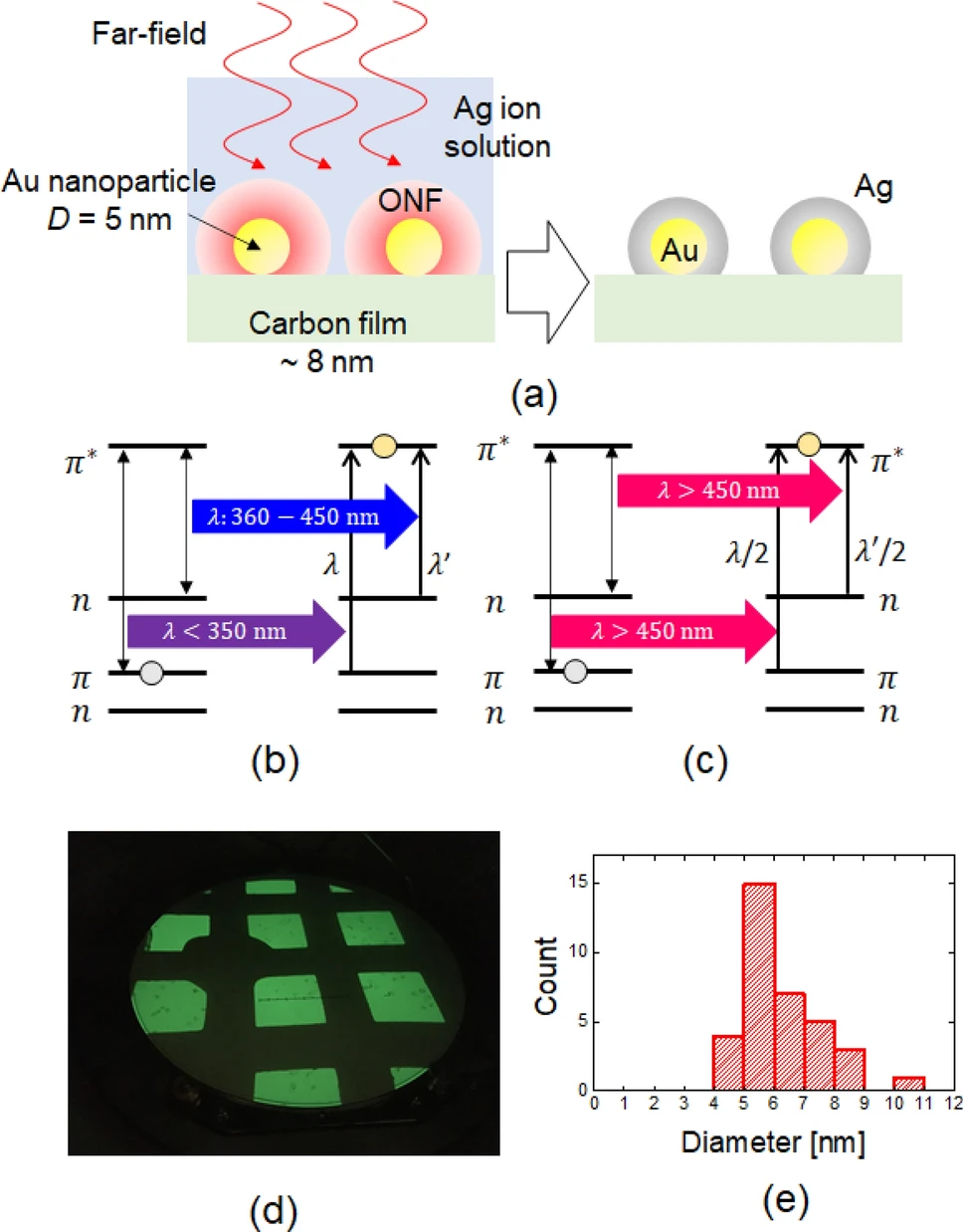
Synthesis of silver nanostructure on gold nanoparticle using near field assisted second harmonic generation Journal Article
In: Scientific Reports, vol. 11, pp. 5642, 2021.
Abstract | Links | BibTeX | タグ: First, Nanophotonic fabrication, Near-field effect, SHG
@article{ag21,

title = {Synthesis of silver nanostructure on gold nanoparticle using near field assisted second harmonic generation},

author = {Takashi Yatsui and Felix Brandenburg and Benjamin Leuschel and Olivier Soppera},

doi = {10.1038/s41598-021-84944-w},

year  = {2021},

date = {2021-03-11},

urldate = {2021-03-11},

journal = {Scientific Reports},

volume = {11},

pages = {5642},

abstract = {By using gold (Au) nanoparticles (NPs) as an optical near-field source under far-field illumination in combination with a silver (Ag) ion solution containing a photoinitiator, we coated Ag on Au NPs using a near-field (NF)-assisted process. We evaluated the change in the size of the NPs using transmission electron microscopy. Evaluation of the synthesized Ag volume over illumination power confirmed the squared power dependence of the NP volume with illumination using 808 nm light, i.e., a wavelength longer than the absorption edge wavelength of the photoinitiator molecules. The rate of volume increase was much lower than the plasmonic field enhancement effect. Therefore, the squared power dependency of the volume increase using a wavelength longer than the absorption edge wavelength originated from NF-assisted second-harmonic generation and the resulting excitation.},

keywords = {First, Nanophotonic fabrication, Near-field effect, SHG},

pubstate = {published},

tppubtype = {article}

}
2018
Felix Brandenburg, Ryosuke Nagumo, Kota Saichi, Kosuke Tahara, Takayuki Iwasaki, Mutsuko Hatano, Fedor Jelezko, Ryuji Igarashi, Takashi Yatsui
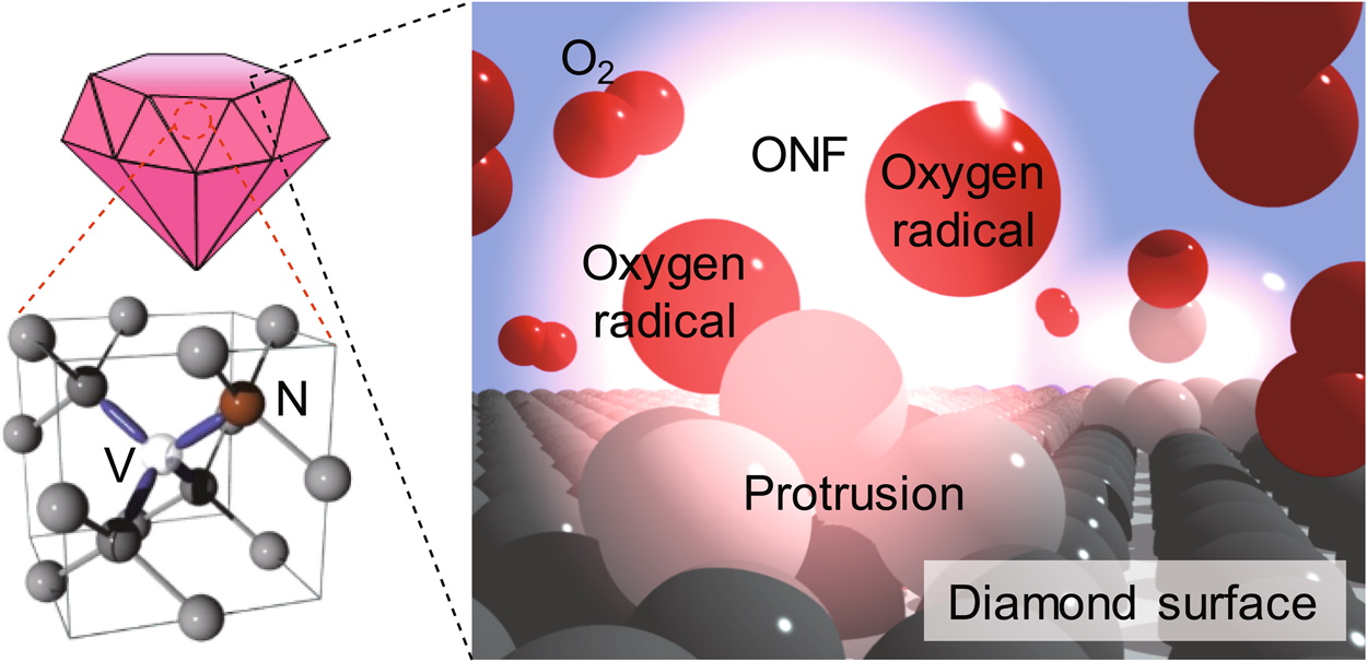
Improving the electron spin properties of nitrogen-vacancy centres in nanodiamonds by near-field etching Journal Article
In: Scientific Reports, vol. 8, pp. 15847, 2018.
Abstract | Links | BibTeX | タグ: Diamond, Nanophotonic fabrication, Near-field etching, NV center
@article{2018Felix,

title = {Improving the electron spin properties of nitrogen-vacancy centres in nanodiamonds by near-field etching},

author = {Felix Brandenburg and Ryosuke Nagumo and Kota Saichi and Kosuke Tahara and Takayuki Iwasaki and Mutsuko Hatano and Fedor Jelezko and Ryuji Igarashi and Takashi Yatsui},

doi = {10.1038/s41598-018-34158-4},

year  = {2018},

date = {2018-10-01},

urldate = {2018-10-01},

journal = {Scientific Reports},

volume = {8},

pages = {15847},

publisher = {Springer Nature},

abstract = {The nitrogen-vacancy (NV) centre in diamond is a promising candidate for quantum computing applications and magnetic sensing applications, because it is an atomic-scale defect with stable coherence time (T2) and reliable accessibility at room temperature. We demonstrated a method for improving the NV spin properties (the full width half maximum (FWHM) value of the magnetic resonance spectrum and T2) through a near-field (NF) etching method under ambient conditions. The NF etching method, based on a He-Cd ultraviolet laser (325 nm), which is longer than the absorption edge of the oxygen molecule, enabled selective removal of defects on the nanodiamond surface. We observed a decrease in the FWHM value close to 15% and an increase in T2 close to 25%. Since our technique can be easily reproduced, a wide range of NV centre applications could be improved, especially magnetic sensing applications. Our results are especially attractive, because they have been obtained under ambient conditions and only require a light source with wavelength slightly above the O2 absorption edge.},

keywords = {Diamond, Nanophotonic fabrication, Near-field etching, NV center},

pubstate = {published},

tppubtype = {article}

}
2017
Takashi Yatsui, Hiroshi Saito, Katsuhiro Nishioka, Benjamin Leuschel, Olivier Soppera, Katsuyuki Nobusada
Effects of a power and photon energy of incident light on near-field etching properties Journal Article
In: Applied Physics A, vol. 123, no. 12, pp. 751, 2017.
Abstract | Links | BibTeX | タグ: First, Nanophotonic fabrication, Near-field etching
@article{2017yatsuiAPA,

title = {Effects of a power and photon energy of incident light on near-field etching properties},

author = {Takashi Yatsui and Hiroshi Saito and Katsuhiro Nishioka and Benjamin Leuschel and Olivier Soppera and Katsuyuki Nobusada},

doi = {10.1007/s00339-017-1361-z},

year  = {2017},

date = {2017-12-01},

journal = {Applied Physics A},

volume = {123},

number = {12},

pages = {751},

publisher = {Springer Nature},

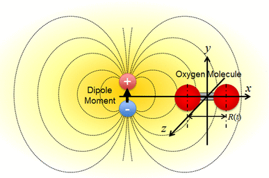
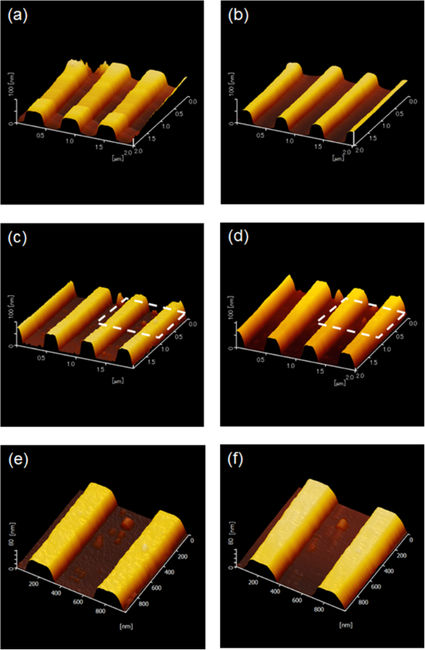
abstract = {We developed a near-field etching technique for realizing an ultra-flat surfaces of various materials and structures. To elucidate the near-field etching properties, we have investigated the effects of power and the photon energy of the incident light. First, we established theoretically that an optical near-field with photon energy lower than the absorption edge of the molecules can induce molecular vibrations. We used nanodiamonds to study the power dependence of the near-field etching properties. From the topological changes of the nanodiamonds, we confirmed the linear-dependence of the etching volume with the incident power. Furthermore, we studied the photon energy dependence using TiO2 nanostriped structures, which revealed that a lower photon energy results in a lower etching rate.},

keywords = {First, Nanophotonic fabrication, Near-field etching},

pubstate = {published},

tppubtype = {article}

}
Takashi Yatsui, Hiroshi Saito, Katsuyuki Nobusada
Angstrom-scale flatness using selective nanoscale etching Journal Article
In: Beilstein Journal of Nanotechnology, vol. 123, pp. 751, 2017.
Abstract | Links | BibTeX | タグ: First, Nanophotonic fabrication, Near-field etching, Wet etching
@article{2017yatsuiBJ,

title = {Angstrom-scale flatness using selective nanoscale etching},

author = {Takashi Yatsui and Hiroshi Saito and Katsuyuki Nobusada},

doi = {10.3762/bjnano.8.217},

year  = {2017},

date = {2017-10-01},

journal = {Beilstein Journal of Nanotechnology},

volume = {123},

pages = {751},

publisher = {Beilstein-Institut.},

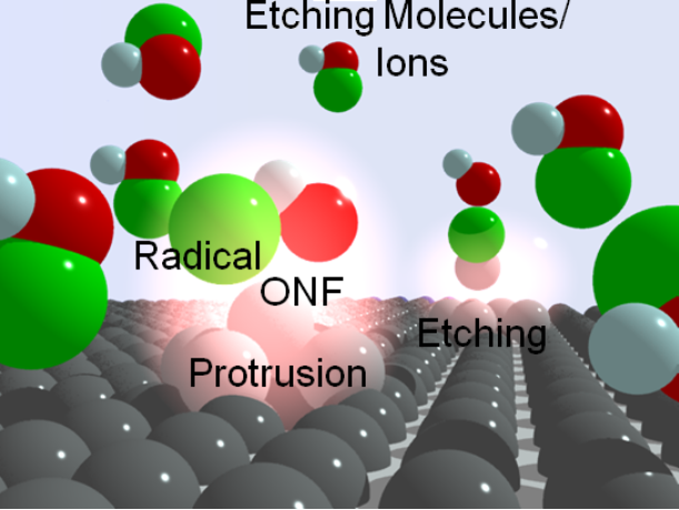
abstract = {The realization of flat surfaces on the angstrom scale is required in advanced devices to avoid loss due to carrier (electron and/or photon) scattering. In this work, we have developed a new surface flattening method that involves near-field etching, where optical near-fields (ONFs) act to dissociate the molecules. ONFs selectively generated at the apex of protrusions on the surface selectively etch the protrusions. To confirm the selective etching of the nanoscale structure, we compared near-field etching using both gas molecules and ions in liquid phase. Using two-dimensional Fourier analysis, we found that near-field etching is an effective way to etch on the scale of less than 10 nm for both wet and dry etching techniques. In addition, near-field dry etching may be effective for the selective etching of nanoscale structures with large mean free path values.},

keywords = {First, Nanophotonic fabrication, Near-field etching, Wet etching},

pubstate = {published},

tppubtype = {article}

}
Felix Brandenburg, Tomohiro Okamoto, Hiroshi Saito, Benjamin Leuschel, Olivier Soppera, Takashi Yatsui
Surface improvement of organic photoresists using a near-field-dependent etching method Journal Article
In: Beilstein Journal of Nanotechnology, vol. 8, pp. 784-788, 2017.
Abstract | Links | BibTeX | タグ: Nanophotonic fabrication, Near-field etching
@article{2017FelixBJ,

title = {Surface improvement of organic photoresists using a near-field-dependent etching method},

author = {Felix Brandenburg and Tomohiro Okamoto and Hiroshi Saito and Benjamin Leuschel and Olivier Soppera and Takashi Yatsui},

doi = {10.3762/bjnano.8.81},

year  = {2017},

date = {2017-04-01},

journal = {Beilstein Journal of Nanotechnology},

volume = {8},

pages = {784-788},

publisher = {Beilstein-Institut.},

abstract = {Surface flattening techniques are extremely important for the development of future electrical and/or optical devices because carrier-scattering losses due to surface roughness severely limit the performance of nanoscale devices. To address the problem, we have developed a near-field etching technique that provides selective etching of surface protrusions, resulting in an atomically flat surface. To achieve finer control, we examine the importance of the wavelength of the near-field etching laser. Using light sources at wavelengths of 325 and 405 nm, which are beyond the absorption edge of the photoresist (310 nm), we compare the resulting cross-sectional etching volumes. The volumes were larger when 325 nm light was employed, i.e., closer to the absorption edge. Although 405 nm light did not cause structural change in the photoresist, a higher reduction of the surface roughness was observed as compared to the 325 nm light. These results indicate that even wavelengths above 325 nm can cause surface roughness improvements without notably changing the structure of the photoresist.},

keywords = {Nanophotonic fabrication, Near-field etching},

pubstate = {published},

tppubtype = {article}

}
2016
Takashi Yatsui, Toshiki Tsuboi, Maiku Yamaguchi, Katsuyuki Nobusada, Satoshi Tojo, Fabrice Stehlin, Olivier Soppera, Daniel Bloch
Optically controlled magnetic-field etching on the nano-scale Journal Article
In: Light: Science & Applications, vol. 5, pp. e16054, 2016.
Abstract | Links | BibTeX | タグ: First, Nanophotonic fabrication, Near-field etching, Selected
@article{2016YatsuiLST,

title = {Optically controlled magnetic-field etching on the nano-scale},

author = {Takashi Yatsui and Toshiki Tsuboi and Maiku Yamaguchi and Katsuyuki Nobusada and Satoshi Tojo and Fabrice Stehlin and Olivier Soppera and Daniel Bloch},

url = {https://www.altmetric.com/details/6399772},

doi = {10.1038/lsa.2016.54},

year  = {2016},

date = {2016-03-25},

journal = {Light: Science & Applications},

volume = {5},

pages = {e16054},

publisher = {Springer Nature},

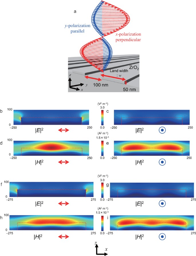
abstract = {Electric and magnetic fields play an important role in both chemical and physical reactions. However, since the coupling efficiency between magnetic fields and electrons is low in comparison with that between electric fields and electrons in the visible wavelength region, the magnetic field is negligible in photo-induced reactions. Here, we performed photo-etching of ZrO2 nano-stripe structures, and identified an etching-property polarisation dependence. Specifically, the etching rate and etched profiles depend on the structure width. To evaluate this polarisation-dependent etching, we performed numerical calculations using a finite-difference time-domain method. Remarkably, the numerical results revealed that the polarisation-dependent etching properties were determined by the magnetic field distributions, rather than the electric field distributions. As nano-scale structures induce a localised magnetic field, the discovery of this etching dependence on the magnetic field is expected to introduce a new perspective on advanced nano-scale structure fabrication.},

keywords = {First, Nanophotonic fabrication, Near-field etching, Selected},

pubstate = {published},

tppubtype = {article}

}
2015
Wataru Nomura, Takashi Yatsui, Tadashi Kawazoe, Naoya Tate, Motoichi Ohtsu
High-speed flattening of crystallized glass substrates by dressed-photon-phonon etching Journal Article
In: Applied Physics A, vol. 121, no. 4, pp. 1403-1407, 2015.
Abstract | Links | BibTeX | タグ: Nanophotonic fabrication, Near-field etching
@article{2015NomuraAPA,

title = {High-speed flattening of crystallized glass substrates by dressed-photon-phonon etching},

author = {Wataru Nomura and Takashi Yatsui and Tadashi Kawazoe and Naoya Tate and Motoichi Ohtsu},

doi = {10.1007/s00339-015-9466-8},

year  = {2015},

date = {2015-12-01},

journal = {Applied Physics A},

volume = {121},

number = {4},

pages = {1403-1407},

publisher = {Springer Nature},

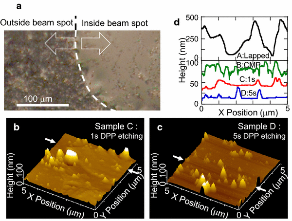
abstract = {Dressed-photon-phonon (DPP) etching is a non-contact flattening technology that realizes ultra-flat surfaces and has been reported to achieve an arithmetic mean surface roughness, R a, on the order of 0.1 nm in various materials, such as fused silica, plastic films, and GaN crystal. In this study, we successfully flattened the surface of a crystallized glass substrate in several seconds using laser light with a higher power density than that used in previous studies. The target substrate had an initial appearance similar to frosted glass, with an R a of 92.5 nm. We performed DPP etching under a Cl2 atmosphere using a CW laser with a wavelength of 532 nm, a power of 8 W, and a spot diameter of 0.2 mm. After 1 s of processing, we obtained a flat surface with an R a of 5.00 nm. This surface roughness equaled or surpassed that of a substrate flattened by conventional chemical mechanical polishing, with an R a of 5.77 nm. Through the detailed analysis of atomic force microscopic images, we found the DPP etching resulted in the smaller standard deviation of the height difference than CMP in the smaller lateral size than 50 nm.},

keywords = {Nanophotonic fabrication, Near-field etching},

pubstate = {published},

tppubtype = {article}

}
Ryosuke Nagumo, Felix Brandenburg, Anna Ermakova, Fedor Jelezko, Takashi Yatsui
Spectral control of nanodiamond using dressed photon-phonon etching Journal Article
In: Applied Physics A, vol. 121, no. 4, pp. 1335-1339, 2015.
Abstract | Links | BibTeX | タグ: Diamond, Nanophotonic fabrication, Near-field etching, NV center
@article{2015NagumoAPA,

title = {Spectral control of nanodiamond using dressed photon-phonon etching},

author = {Ryosuke Nagumo and Felix Brandenburg and Anna Ermakova and Fedor Jelezko and Takashi Yatsui},

doi = {10.1007/s00339-015-9400-0},

year  = {2015},

date = {2015-12-01},

journal = {Applied Physics A},

volume = {121},

number = {4},

pages = {1335-1339},

publisher = {Springer Nature},

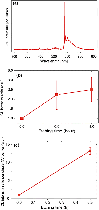
abstract = {The luminescence of a nitrogen-vacancy (NV) center in a nanodiamond (ND) is of great interest because of its features, especially in the field of nanophotonics. When an NV center in an ND is located in the vicinity of the surface, the emission is often disturbed by any surface defects, resulting in non-radiative recombination. In this work, we performed dressed photon-phonon (DPP) etching of the NDs, and found that the size of the NDs decreased, while the cathodoluminescence (CL) intensity increased. We assume that this increase in the CL intensity originates from the removal of the surface protrusions and/or defects by DPP etching.},

keywords = {Diamond, Nanophotonic fabrication, Near-field etching, NV center},

pubstate = {published},

tppubtype = {article}

}
Maiku Yamaguchi, Katsuyuki Nobusada, Tadashi Kawazoe, Takashi Yatsui
Two-photon absorption induced by electric field gradient of optical near-field and its application to photolithography Journal Article
In: Applied Physics Letters, vol. 106, no. 19, pp. 191103, 2015.
Abstract | Links | BibTeX | タグ: Nanophotonic fabrication, Non-uniform optical near field, SHG
@article{2015SHG,

title = {Two-photon absorption induced by electric field gradient of optical near-field and its application to photolithography},

author = {Maiku Yamaguchi and Katsuyuki Nobusada and Tadashi Kawazoe and Takashi Yatsui},

doi = {10.1063/1.4921005},

year  = {2015},

date = {2015-05-01},

urldate = {2015-05-01},

journal = {Applied Physics Letters},

volume = {106},

number = {19},

pages = {191103},

abstract = {An electric field gradient is an inherent property of the optical near-field (ONF). We investigated its effect on electron excitation in a quantum dot via model calculations combining a density matrix formalism and a classical Lorentz model. The electric field gradient of the ONF was found to cause two-photon absorption by an unusual mechanism. Furthermore, the absorption exhibits a nonmonotonic dependence on the spatial arrangement of the nanosystem, completely different from that of conventional two-photon absorption induced by an intense electric field. The present two-photon absorption process was verified in a previous experimental observation by reinterpreting the results of ONF photolithography.},

keywords = {Nanophotonic fabrication, Non-uniform optical near field, SHG},

pubstate = {published},

tppubtype = {article}

}
Takashi Yatsui, Wataru Nomura, Motoichi Ohtsu
Realization of Ultraflat Plastic Film Using Dressed-Photon-Phonon-Assisted Selective Etching of Nanoscale Structures Journal Article
In: Advances in Optical Technologies, vol. 2015, pp. 701802, 2015.
Abstract | Links | BibTeX | タグ: First, Nanophotonic fabrication, Near-field etching
@article{2015Plastic,

title = {Realization of Ultraflat Plastic Film Using Dressed-Photon-Phonon-Assisted Selective Etching of Nanoscale Structures},

author = {Takashi Yatsui and Wataru Nomura and Motoichi Ohtsu},

doi = {10.1155/2015/701802},

year  = {2015},

date = {2015-02-01},

urldate = {2015-02-01},

journal = {Advances in Optical Technologies},

volume = {2015},

pages = {701802},

abstract = {We compared dressed-photon-phonon (DPP) etching to conventional photochemical etching and, using a numerical analysis of topographic images of the resultant etched polymethyl methacrylate (PMMA) substrate, we determined that the DPP etching resulted in the selective etching of smaller scale structures in comparison with the conventional photochemical etching. We investigated the wavelength dependence of the PMMA substrate etching using an O2 gas. As the dissociation energy of O2 is 5.12 eV, we applied a continuous-wave (CW) He-Cd laser ( 325 nm, 3.81 eV) for the DPP etching and a 5th-harmonic Nd:YAG laser (213  nm, 5.82 eV) for the conventional photochemical etching. From the obtained atomic force microscope images, we confirmed a reduction in surface roughness, Ra, in both cases. However, based on calculations involving the standard deviation of the height difference function, we confirmed that the conventional photochemical etching method etched the larger scale structures only, while the DPP etching process selectively etched the smaller scale features.},

keywords = {First, Nanophotonic fabrication, Near-field etching},

pubstate = {published},

tppubtype = {article}

}
2014
Takashi Yatsui, Fumihiro Morigaki, Tadashi Kawazoe
Controlling the optical and structural properties of ZnS-AgInS2 nanocrystals using photo-induced process Journal Article
In: Beilstein Journal of Nanotechnology, vol. 5, pp. 1767-1773, 2014.
Abstract | Links | BibTeX | タグ: First, Nanophotonic fabrication, ZAIS
@article{2014ZAISBJ,

title = {Controlling the optical and structural properties of ZnS-AgInS2 nanocrystals using photo-induced process},

author = {Takashi Yatsui and Fumihiro Morigaki and Tadashi Kawazoe},

doi = {10.3762/bjnano.5.187},

year  = {2014},

date = {2014-10-01},

journal = {Beilstein Journal of Nanotechnology},

volume = {5},

pages = {1767-1773},

publisher = {Beilstein-Institut.},

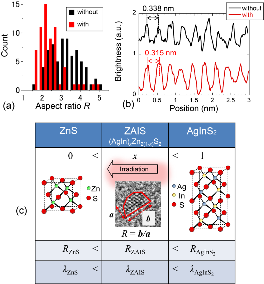
abstract = {ZnS-AgInS2 (ZAIS) solid-solution nanocrystals are promising materials for nanophotonic devices in the visible region because of their low toxicity and good emission properties. We developed a technique of photo-induced synthesis to control the size and composition of the ZAIS nanocrystals. This method successfully decreased the defect levels, as well as the size and size variation of ZAIS nanocrystals by controlling the excitation wavelength during synthesis. Detailed analysis of transmission electron microscope images confirmed that the photo-induced synthesis yielded a high crystallinity of the ZAIS nanocrystals with small variations in size and content.},

keywords = {First, Nanophotonic fabrication, ZAIS},

pubstate = {published},

tppubtype = {article}

}
Hac Huong Thu Le, Kazuma Mawatari, Yuriy Pihosh, Tadashi Kawazoe, Takashi Yatsui, Motoichi Ohtsu, Takehiko Kitamori
Novel sub-100 nm surface chemical modification by optical near-field induced photocatalytic reaction Journal Article
In: Microfluidics and Nanofluidics, vol. 17, no. 4, pp. 751-758, 2014.
Abstract | Links | BibTeX | タグ: Nanophotonic fabrication, Near-field effect, Photocatalytic reaction
@article{2014Le,

title = {Novel sub-100 nm surface chemical modification by optical near-field induced photocatalytic reaction},

author = {Hac Huong Thu Le and Kazuma Mawatari and Yuriy Pihosh and Tadashi Kawazoe and Takashi Yatsui and Motoichi Ohtsu and Takehiko Kitamori},

doi = {10.1007/s10404-014-1361-7},

year  = {2014},

date = {2014-10-01},

journal = {Microfluidics and Nanofluidics},

volume = {17},

number = {4},

pages = {751-758},

publisher = {Springer Nature},

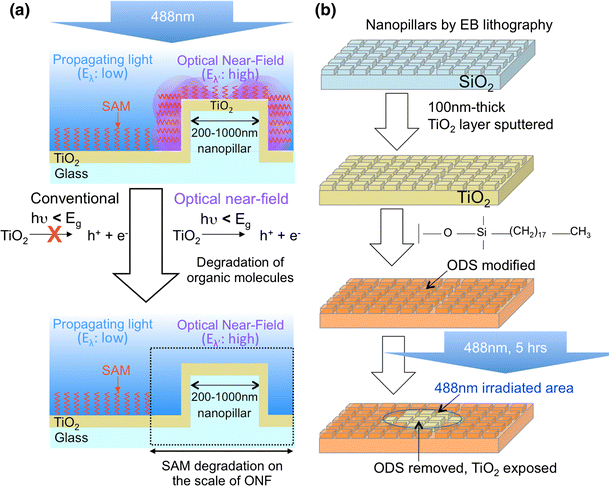
abstract = {The surface modification is indispensable to facilitate new functional applications of micro/nanofluidics devices. Among many modification techniques developed so far, the photo-induced chemical modification is the most versatile method in terms of robustness, process simplicity, and feasibility of chemical functionality. In particular, the method is useful for closed spaces, such as post-bonded devices. However, the limitation by optical diffraction limit is still a challenging issue in scaling down the pattern sizes to nanoscale. Here, we demonstrated a novel surface modification on sub-100 nm scale utilizing the novel optical near-field (ONF) generated on nanostructures of photocatalyst (TiO2). The minimum pattern size of 40 nm, which was much smaller than diffraction limit, was achieved using a visible light source (488 nm) and a conventional irradiation setup. The controllability of pattern size by light intensity, the feasibility of functionality, and the non-contact working mode have impacts on surface patterning of post-bonded micro/nanofluidics devices. It is also worthy to note that our results verified for the first time the ONF on nanostructures of non-metal materials and its ability to manipulate the chemical reaction on nanoscale.},

keywords = {Nanophotonic fabrication, Near-field effect, Photocatalytic reaction},

pubstate = {published},

tppubtype = {article}

}
Takashi Yatsui, Daisuke Takeuchi, Satoshi Koizumi, Kazuki Sato, Kohei Tsuzuki, Takayuki Iwasaki, Mutsuko Hatano, Toshiharu Makino, Masahiko Ogura, Hiromitsu Kato, Hideyo Okushi, Satoshi Yamasaki
Polarization-controlled dressed-photon–phonon etching of patterned diamond structures Journal Article
In: physica status solidi (a), vol. 211, no. 10, pp. 2339-2342, 2014.
Abstract | Links | BibTeX | タグ: Diamond, First, Nanophotonic fabrication, Near-field etching
@article{doi:10.1002/pssa.201431161,

title = {Polarization-controlled dressed-photon–phonon etching of patterned diamond structures},

author = {Takashi Yatsui and Daisuke Takeuchi and Satoshi Koizumi and Kazuki Sato and Kohei Tsuzuki and Takayuki Iwasaki and Mutsuko Hatano and Toshiharu Makino and Masahiko Ogura and Hiromitsu Kato and Hideyo Okushi and Satoshi Yamasaki},

doi = {10.1002/pssa.201431161},

year  = {2014},

date = {2014-10-01},

journal = {physica status solidi (a)},

volume = {211},

number = {10},

pages = {2339-2342},

abstract = {To realize an ultra-flat diamond surface with a three-dimensional (3D) structure, we performed dressed-photon–phonon (DPP) etching. A DPP is generated on nano-scale protrusions. Hence, the generation of DPPs results in selective removal of nano-scale protrusions, thereby achieving an ultra-flat surface even on the sidewall of a diamond mesa structure. By controlling the polarization of the incident light, a smooth diamond mesa structure sidewall was obtained, and a higher etching rate was obtained with a perpendicular polarization on the corrugations. In addition, by selective deposition of n-layer diamond on the p-layer diamond mesa structure, smooth n-layer diamond was confirmed on the DPP etched sidewall. Schematic of dressed-photon–phonon (DPP) etching on the sidewall: (a) before and (b) after etching, in which DPP selectively generates on the corrugations and etching automatically stops when the surface was smooth. Scanning electron microscopy image of the selective deposition of the n-layer (c) without and (d) with the DPP etched sidewall.},

keywords = {Diamond, First, Nanophotonic fabrication, Near-field etching},

pubstate = {published},

tppubtype = {article}

}
Wataru Nomura, Tadashi Kawazoe, Takashi Yatsui, Makoto Naruse, Motoichi Ohtsu
In: Beilstein Journal of Nanotechnology, vol. 5, pp. 1334-1340, 2014.
Abstract | Links | BibTeX | タグ: Nanophotonic fabrication, Near-field etching
@article{2014ZAISBJb,
title = {Observation and analysis of structural changes in fused silica by continuous irradiation with femtosecond laser light having an energy density below the laser-induced damage threshold},
author = {Wataru Nomura and Tadashi Kawazoe and Takashi Yatsui and Makoto Naruse and Motoichi Ohtsu},
doi = {10.3762/bjnano.5.146},
year = {2014},
date = {2014-08-01},
journal = {Beilstein Journal of Nanotechnology},
volume = {5},
pages = {1334-1340},
publisher = {Beilstein-Institut.},
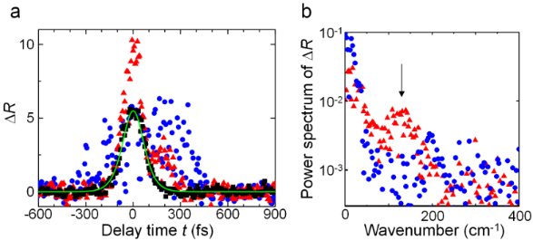
abstract = {The laser-induced damage threshold (LIDT) is widely used as an index for evaluating an optical componentfs resistance to laser light. However, a degradation in the performance of an optical component is also caused by continuous irradiation with laser light having an energy density below the LIDT. Therefore, here we focused on the degradation in performance of an optical component caused by continuous irradiation with femtosecond laser light having a low energy density, i.e., laser-induced degradation. We performed an in situ observation and analysis of an increase in scattering light intensity in fused silica substrates. In experiments conducted using a pulsed laser with a wavelength of 800 nm, a pulse width of 160 fs and pulse repetition rate of 1 kHz, we found that the scattered light intensity increased starting from a specific accumulated fluence, namely, that the laser-induced degradation had a threshold. We evaluated the threshold fluence Ft as 6.27 J/cm2 and 9.21 J/cm2 for the fused silica substrates with surface roughnesses of 0.20 nm and 0.13 nm in Ra value, respectively, showing that the threshold decreased as the surface roughness increased. In addition, we found that the reflected light spectrum changed as degradation proceeded. We analyzed the details of the degradation by measuring instantaneous reflectance changes with a pump-probe method; we observed an increase in the generation probability of photogenerated carriers in a degraded silica substrate and a damaged silica substrate and observed a Raman signal originating from a specific molecular structure of silica. From these findings, we concluded that compositional changes in the molecular structure occurred during degradation due to femtosecond laser irradiation having an energy density below the LIDT.},
keywords = {Nanophotonic fabrication, Near-field etching},
pubstate = {published},
tppubtype = {article}
}
2013
Takashi Yatsui, Wataru Nomura, Fabrice Stehlin, Olivier Soppera, Makoto Naruse, Motoichi Ohtsu
Challenge in realizing ultraflat material surfaces Journal Article
In: Beilstein Journal of Nanotechnology, vol. 4, pp. 875-885, 2013, (review article).
Abstract | Links | BibTeX | タグ: First, Nanophotonic fabrication, Near-field etching, Review, Selected
@article{2013yatsuiBJrev,
title = {Challenge in realizing ultraflat material surfaces},
author = {Takashi Yatsui and Wataru Nomura and Fabrice Stehlin and Olivier Soppera and Makoto Naruse and Motoichi Ohtsu},
doi = {10.3762/bjnano.4.99},
year = {2013},
date = {2013-12-01},
journal = {Beilstein Journal of Nanotechnology},
volume = {4},
pages = {875-885},
publisher = {Beilstein-Institut.},
abstract = {The laser-induced damage threshold (LIDT) is widely used as an index for evaluating an optical componentfs resistance to laser light. However, a degradation in the performance of an optical component is also caused by continuous irradiation with laser light having an energy density below the LIDT. Therefore, here we focused on the degradation in performance of an optical component caused by continuous irradiation with femtosecond laser light having a low energy density, i.e.Ultraflat surface substrates are required to achieve an optimal performance of future optical, electronic, or optoelectronic devices for various applications, because such surfaces reduce the scattering loss of photons, electrons, or both at the surfaces and interfaces. In this paper, we review recent progress toward the realization of ultraflat materials surfaces. First, we review the development of surface-flattening techniques. Second, we briefly review the dressed photon-phonon (DPP), a nanometric quasiparticle that describes the coupled state of a photon, an electron, and a multimode-coherent phonon. Then, we review several recent developments based on DPP-photochemical etching and desorption processes, which have resulted in angstrom-scale flat surfaces. To confirm that the superior flatness of these surfaces that originated from the DPP process, we also review a simplified mathematical model that describes the scale-dependent effects of optical near-fields. Finally, we present the future outlook for these technologies.},
note = {review article},
keywords = {First, Nanophotonic fabrication, Near-field etching, Review, Selected},
pubstate = {published},
tppubtype = {article}
}
Naoya Tate, Makoto Naruse, Yang Liu, Tadashi Kawazoe, Takashi Yatsui, Motoichi Ohtsu
Experimental demonstration and stochastic modeling of autonomous formation of nanophotonic droplets Journal Article
In: Applied Physics B, vol. 112, no. 4, pp. 587-592, 2013.
Abstract | Links | BibTeX | タグ: Droplet, Nanophotonic fabrication, Near-field effect
@article{2013tateAPB3,

title = {Experimental demonstration and stochastic modeling of autonomous formation of nanophotonic droplets},

author = {Naoya Tate and Makoto Naruse and Yang Liu and Tadashi Kawazoe and Takashi Yatsui and Motoichi Ohtsu},

doi = {10.1007/s00340-013-5442-1},

year  = {2013},

date = {2013-09-01},

journal = {Applied Physics B},

volume = {112},

number = {4},

pages = {587-592},

publisher = {Springer Nature},

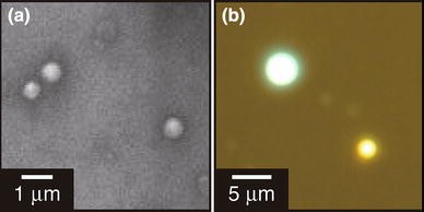
abstract = {We have previously demonstrated a novel technique for autonomously forming a nanophotonic droplet, which is micro-scale spherical polymer structure that contains paired heterogeneous nanometric components. The sort-selectivity and alignment accuracy of the nanometric components in each nanophotonic droplet, and the related homogeneity of the optical function, are due to a characteristic pairing process based on a phonon-assisted photo-curing method. The proposed method requires irradiating a mixture of components with light to induce optical near-field interactions between each component, and subsequent processes based on these interactions. The pairing yield of components via the interactions is considered to mainly depend on the frequency of their encounters and the size-resonance effect between encountered components. In this paper, we model these two factors by individual stochastic procedures and construct a numerical model to describe the pairing process. Agreement between the results of numerical and experimental demonstrations shows the validity of our stochastic modeling.},

keywords = {Droplet, Nanophotonic fabrication, Near-field effect},

pubstate = {published},

tppubtype = {article}

}
Naoya Tate, Yang Liu, Tadashi Kawazoe, Makoto Naruse, Takashi Yatsui, Motoichi Ohtsu
Nanophotonic droplet: a nanometric optical device consisting of size- and number-selective coupled quantum dots Journal Article
In: Applied Physics B, vol. 110, no. 3, pp. 293-297, 2013.
Abstract | Links | BibTeX | タグ: Droplet, Nanophotonic fabrication
@article{2013tateAPB2,

title = {Nanophotonic droplet: a nanometric optical device consisting of size- and number-selective coupled quantum dots},

author = {Naoya Tate and Yang Liu and Tadashi Kawazoe and Makoto Naruse and Takashi Yatsui and Motoichi Ohtsu},

doi = {10.1007/s00340-012-5285-1},

year  = {2013},

date = {2013-03-01},

journal = {Applied Physics B},

volume = {110},

number = {3},

pages = {293-297},

publisher = {Springer Nature},

abstract = {Although recent advances in fabrication technologies have allowed the realization of highly accurate nanometric devices and systems, most approaches still lack uniformity and mass-production capability sufficient for practical use. We have previously demonstrated a novel technique for autonomously coupling heterogeneous quantum dots to induce particular optical responses based on a simple phonon-assisted photocuring method in which a mixture of quantum dots and photocurable polymer is irradiated with light. The cured polymer sequentially encapsulates coupled quantum dots, forming what we call a nanophotonic droplet. Recently, we found that each quantum dot in the mixture is preferably coupled with other quantum dots of similar size due to a size resonance effect of the optical near-field interactions between them. Moreover, every nanophotonic droplet is likely to contain the same number of coupled quantum dots. In this paper, we describe the basic mechanisms of autonomously fabricating nanophotonic droplets, and we examine the size- and number-selectivity of the quantum dots during their coupling process. The results from experiments show the uniformity of the optical properties of mass-produced nanophotonic droplets, revealed by emission from the contained coupled quantum dots, due to the fundamental characteristics of our method.},

keywords = {Droplet, Nanophotonic fabrication},

pubstate = {published},

tppubtype = {article}

}
Naoya Tate, Yang Liu, Tadashi Kawazoe, Makoto Naruse, Takashi Yatsui, Motoichi Ohtsu
Fixed-distance coupling and encapsulation of heterogeneous quantum dots using phonon-assisted photo-curing Journal Article
In: Applied Physics B, vol. 110, no. 1, pp. 39-45, 2013.
Abstract | Links | BibTeX | タグ: Droplet, Nanophotonic fabrication
@article{2013tateAPB1,

title = {Fixed-distance coupling and encapsulation of heterogeneous quantum dots using phonon-assisted photo-curing},

author = {Naoya Tate and Yang Liu and Tadashi Kawazoe and Makoto Naruse and Takashi Yatsui and Motoichi Ohtsu},

doi = {10.1007/s00340-012-5249-5},

year  = {2013},

date = {2013-01-01},

journal = {Applied Physics B},

volume = {110},

number = {1},

pages = {39-45},

publisher = {Springer Nature},

abstract = {We propose a novel method of coupling heterogeneous quantum dots at fixed distances and capsulating the coupled quantum dots by utilizing nanometric local curing of a photo-curable polymer caused by multistep electronic transitions based on a phonon-assisted optical near-field process between quantum dots. Because the coupling and the capsulating processes are triggered only when heterogeneous quantum dots floating in a solution closely approach each other to induce optical near-field interactions between them, the distances between the coupled quantum dots are physically guaranteed to be equal to the scale of the optical near fields. To experimentally verify our idea, we fabricated coupled quantum dots, consisting of CdSe and ZnO quantum dots and a UV-curable polymer. We also measured the photoluminescence properties due to the quantum-dot coupling and showed that the individual photoluminescences from the CdSe and ZnO quantum dots exhibited a trade-off relationship.},

keywords = {Droplet, Nanophotonic fabrication},

pubstate = {published},

tppubtype = {article}

}
2012
Takashi Yatsui, Wataru Nomura, Makoto Naruse, Motoichi Ohtsu
Realization of an atomically flat surface of diamond using dressed photon–phonon etching Journal Article
In: Journal of Physics D: Applied Physics, vol. 45, no. 47, pp. 475302, 2012.
Abstract | Links | BibTeX | タグ: Diamond, First, Nanophotonic fabrication, Near-field etching
@article{Yatsui_2012,

title = {Realization of an atomically flat surface of diamond using dressed photon–phonon etching},

author = {Takashi Yatsui and Wataru Nomura and Makoto Naruse and Motoichi Ohtsu},

url = {https://doi.org/10.1088%2F0022-3727%2F45%2F47%2F475302},

doi = {10.1088/0022-3727/45/47/475302},

year  = {2012},

date = {2012-11-01},

journal = {Journal of Physics D: Applied Physics},

volume = {45},

number = {47},

pages = {475302},

publisher = {IOP Publishing},

abstract = {We obtained an atomically flat diamond surface following dressed photon–phonon (DPP) etching using 3.81 eV light and O2 gas. We obtained a surface roughness (Ra) of 0.154 nm for Ib-type (1 1 1) diamond and 0.096 nm for Ib-type (1 0 0) diamond. To evaluate the surface roughness, we grouped the surface into bins of width l and introduced the standard deviation of the height difference function for a given separation l, which allowed us to determine the height variation of the surface. Based on the calculation of standard deviation, the conventional adiabatic photochemical reaction did not remove the small surface features, while DPP etching decreased the surface roughness for all length scales.},

keywords = {Diamond, First, Nanophotonic fabrication, Near-field etching},

pubstate = {published},

tppubtype = {article}

}
Pham Nam Hai, Wataru Nomura, Takashi Yatsui, Motoichi Ohtsu, Masaaki Tanaka
Effects of laser irradiation on the self-assembly of MnAs nanoparticles in a GaAs matrix Journal Article
In: Applied Physics Letters, vol. 101, no. 19, pp. 193102, 2012.
Abstract | Links | BibTeX | タグ: Nanoparticle, Nanophotonic fabrication, Near-field effect
@article{doi:10.1063/1.4765355,

title = {Effects of laser irradiation on the self-assembly of MnAs nanoparticles in a GaAs matrix},

author = {Pham Nam Hai and Wataru Nomura and Takashi Yatsui and Motoichi Ohtsu and Masaaki Tanaka},

doi = {10.1063/1.4765355},

year  = {2012},

date = {2012-10-01},

urldate = {2012-10-01},

journal = {Applied Physics Letters},

volume = {101},

number = {19},

pages = {193102},

abstract = {We investigate the effects of laser irradiation on the self-assembly of MnAs nanoparticles during solid-phase decomposition in a GaAs matrix. It is found that laser irradiation suppresses the growth of MnAs nanoparticles from small to large size, and that the median diameter D1 in the size distribution of small MnAs nanoparticles depends on the incident photon energy E following D1 ∼ E−1/5. We explain this behavior by the desorption of Mn atoms on the MnAs nanoparticle surface due to resonant optical absorption, in which incident photons excite intersubband electronic transitions between the quantized energy levels in the MnAs nanoparticles.},

keywords = {Nanoparticle, Nanophotonic fabrication, Near-field effect},

pubstate = {published},

tppubtype = {article}

}
Yang Liu, Takashi Yatsui, Motoichi Ohtsu
Controlling the sizes of ZnO quantum dots by using dressed photon-phonon assisted sol-gel method Journal Article
In: Applied Physics B, vol. 108, no. 4, pp. 707-711, 2012.
Abstract | Links | BibTeX | タグ: Nanophotonic fabrication, Near-field effect, QD, Sol-gel, ZnO
@article{2012liuAPB,

title = {Controlling the sizes of ZnO quantum dots by using dressed photon-phonon assisted sol-gel method},

author = {Yang Liu and Takashi Yatsui and Motoichi Ohtsu},

doi = {10.1007/s00340-012-5151-1},

year  = {2012},

date = {2012-09-01},

journal = {Applied Physics B},

volume = {108},

number = {4},

pages = {707-711},

publisher = {Springer Nature},

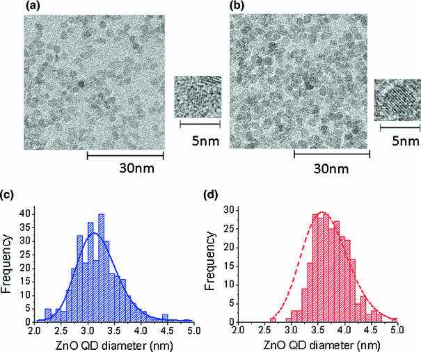
abstract = {We developed a sol-gel method using the dressed photon-phonon (DPP) process. DPPs are selectively exited in nanoscale structures at photon energies that are lower than the bandgap energy, which allows one to increase the growth rate of smaller ZnO quantum dots (QDs). Thus, we obtained a smaller size variance of ZnO QDs. The growth rate was proportional to the power of the light used for DPP excitation. The results were confirmed using a rate equation that accounted for the concentration of the sol-gel solution.},

keywords = {Nanophotonic fabrication, Near-field effect, QD, Sol-gel, ZnO},

pubstate = {published},

tppubtype = {article}

}
2011
Takashi Yatsui, Kazuya Hirata, Yoshinori Tabata, Yumiko Miyake, Yasuyuki Akita, Mamoru Yoshimoto, Wataru Nomura, Tadashi Kawazoe, Makoto Naruse, Motoichi Ohtsu
Self-organized near-field etching of the sidewalls of glass corrugations Journal Article
In: Applied Physics B, vol. 103, no. 3, pp. 527-530, 2011.
Abstract | Links | BibTeX | タグ: First, Nanophotonic fabrication, Near-field etching
@article{2011yatsuiAPBNFE,

title = {Self-organized near-field etching of the sidewalls of glass corrugations},

author = {Takashi Yatsui and Kazuya Hirata and Yoshinori Tabata and Yumiko Miyake and Yasuyuki Akita and Mamoru Yoshimoto and Wataru Nomura and Tadashi Kawazoe and Makoto Naruse and Motoichi Ohtsu},

doi = {10.1007/s00340-011-4569-1},

year  = {2011},

date = {2011-06-01},

journal = {Applied Physics B},

volume = {103},

number = {3},

pages = {527-530},

publisher = {Springer Nature},

abstract = {Using soda-lime glass with a nano-stripe pattern as a test specimen, we demonstrated self-organized near-field etching with a continuum-wave laser (wavelength of 532 nm) light source. Atomic force microscopy confirmed that near-field etching decreases the flank roughness of the corrugations as well as the roughness of the flat surface.},

keywords = {First, Nanophotonic fabrication, Near-field etching},

pubstate = {published},

tppubtype = {article}

}
Yang Liu, Tetsu Morishima, Takashi Yatsui, Tadashi Kawazoe, Motoichi Ohtsu
Size control of sol–gel-synthesized ZnO quantum dots using photo-induced desorption Journal Article
In: Nanotechnology, vol. 22, no. 21, pp. 215605, 2011.
Abstract | Links | BibTeX | タグ: Nanophotonic fabrication, QD, Sol-gel
@article{Liu_2011,

title = {Size control of sol–gel-synthesized ZnO quantum dots using photo-induced desorption},

author = {Yang Liu and Tetsu Morishima and Takashi Yatsui and Tadashi Kawazoe and Motoichi Ohtsu},

doi = {10.1088/0957-4484/22/21/215605},

year  = {2011},

date = {2011-03-01},

journal = {Nanotechnology},

volume = {22},

number = {21},

pages = {215605},

publisher = {IOP Publishing},

abstract = {We developed a sol–gel method using photo-induced desorption for size-controlled ZnO quantum dots (QDs). This method successfully controlled the size and size variance of ZnO QDs, and size fluctuations decreased from 23% to 18% depending on the illuminated light intensity. The sol–gel synthesis effectively reduced the number of defect levels that originated from oxygen defects.},

keywords = {Nanophotonic fabrication, QD, Sol-gel},

pubstate = {published},

tppubtype = {article}

}
2010
Takashi Yatsui, Kazuya Hirata, Yoshinori Tabata, Wataru Nomura, Tadashi Kawazoe, Makoto Naruse, Motoichi Ohtsu
In situ real-time monitoring of changes in the surface roughness during nonadiabatic optical near-field etching Journal Article
In: Nanotechnology, vol. 21, no. 35, pp. 355303, 2010.
Abstract | Links | BibTeX | タグ: First, Nanophotonic fabrication, Near-field etching
@article{Yatsuii_2010,

title = {In situ real-time monitoring of changes in the surface roughness during nonadiabatic optical near-field etching},

author = {Takashi Yatsui and Kazuya Hirata and Yoshinori Tabata and Wataru Nomura and Tadashi Kawazoe and Makoto Naruse and Motoichi Ohtsu},

doi = {10.1088/0957-4484/21/35/355303},

year  = {2010},

date = {2010-08-01},

journal = {Nanotechnology},

volume = {21},

number = {35},

pages = {355303},

publisher = {IOP Publishing},

abstract = {We performed in situ real-time monitoring of the change in surface roughness during

self-organized optical near-field etching. During near-field etching of a silica substrate, we detected the scattered light intensity from a continuum wave (CW) laser (λ = 633 nm) in addition to the etching CW laser (λ = 532 nm) light source. We discovered that near-field etching not only decreases surface

roughness, but also increases the number of scatterers, as was confirmed by analyzing the

AFM image. These approaches provide optimization criteria for the etching parameter and

hence for further decreases in surface roughness.},

keywords = {First, Nanophotonic fabrication, Near-field etching},

pubstate = {published},

tppubtype = {article}

}
self-organized optical near-field etching. During near-field etching of a silica substrate, we detected the scattered light intensity from a continuum wave (CW) laser (λ = 633 nm) in addition to the etching CW laser (λ = 532 nm) light source. We discovered that near-field etching not only decreases surface
roughness, but also increases the number of scatterers, as was confirmed by analyzing the
AFM image. These approaches provide optimization criteria for the etching parameter and
hence for further decreases in surface roughness.
Kokoro Kitamura, Takashi Yatsui, Tadashi Kawazoe, Masakazu Sugiyama, Motoichi Ohtsu
Site-selective deposition of gold nanoparticles using non-adiabatic reaction induced by optical near-fields Journal Article
In: Nanotechnology, vol. 21, no. 28, pp. 285302, 2010.
Abstract | Links | BibTeX | タグ: Nanophotonic fabrication, nanorod, Near-field effect, ZnO
@article{Kitamura_2010,

title = {Site-selective deposition of gold nanoparticles using non-adiabatic reaction induced by optical near-fields},

author = {Kokoro Kitamura and Takashi Yatsui and Tadashi Kawazoe and Masakazu Sugiyama and Motoichi Ohtsu},

doi = {10.1088/0957-4484/21/28/285302},

year  = {2010},

date = {2010-06-01},

journal = {Nanotechnology},

volume = {21},

number = {28},

pages = {285302},

publisher = {IOP Publishing},

abstract = {In this paper, we report on site-selective deposition of metal nanoparticles

using a non-adiabatic photochemical reaction. Photoreduction of gold

was performed in a silica gel membrane containing tetrachloroaurate (AuCl4 − ) ions, using ZnO nanorods as the sources of optical near-field light, resulting in deposition

of gold nanoparticles with an average diameter of 17.7 nm. The distribution of

distances between the gold nanoparticles and nanorod traces revealed that the gold

nanoparticles were deposited adjacent to the ZnO nanorods, reflecting the attenuation of

the optical near-fields in the vicinity of the ZnO nanorods. We found that the

emission wavelength from the ZnO nanorods was longer than the absorption edge

wavelength of the tetrachloroaurate. Additionally, from the intensity distribution

obtained by a finite-difference time-domain method, the gold deposited around the

ZnO nanorods was found to be due to a non-adiabatic photochemical reaction.},

keywords = {Nanophotonic fabrication, nanorod, Near-field effect, ZnO},

pubstate = {published},

tppubtype = {article}

}
using a non-adiabatic photochemical reaction. Photoreduction of gold
was performed in a silica gel membrane containing tetrachloroaurate (AuCl4 − ) ions, using ZnO nanorods as the sources of optical near-field light, resulting in deposition
of gold nanoparticles with an average diameter of 17.7 nm. The distribution of
distances between the gold nanoparticles and nanorod traces revealed that the gold
nanoparticles were deposited adjacent to the ZnO nanorods, reflecting the attenuation of
the optical near-fields in the vicinity of the ZnO nanorods. We found that the
emission wavelength from the ZnO nanorods was longer than the absorption edge
wavelength of the tetrachloroaurate. Additionally, from the intensity distribution
obtained by a finite-difference time-domain method, the gold deposited around the
ZnO nanorods was found to be due to a non-adiabatic photochemical reaction.
Sotaro Yukutake, Tadashi Kawazoe, Takashi Yatsui, Wataru Nomura, Kokoro Kitamura, Motoichi Ohtsu
In: Applied Physics B, vol. 99, no. 3, pp. 415-422, 2010.
Abstract | Links | BibTeX | タグ: Nanophotonic fabrication, Near-field effect, Self-assembly
@article{2010yukutakeAPB,

title = {Selective photocurrent generation in the transparent wavelength range of a semiconductor photovoltaic device using a phonon-assisted optical near-field process},

author = {Sotaro Yukutake and Tadashi Kawazoe and Takashi Yatsui and Wataru Nomura and Kokoro Kitamura and Motoichi Ohtsu},

doi = {10.1007/s00340-010-3999-5},

year  = {2010},

date = {2010-05-01},

journal = {Applied Physics B},

volume = {99},

number = {3},

pages = {415-422},

publisher = {Springer Nature},

abstract = {In this paper, we propose a novel photovoltaic device using P3HT and ZnO as test materials for the ptype and n-type semiconductors, respectively. To fabricate an electrode of this device, Ag was deposited on a P3HT film by RF-sputtering under light illumination (wavelength λ0 = 660 nm) while reversely biasing the P3HT/ZnO pnjunction. As a result, a unique granular Ag film was formed, which originated from a phonon-assisted process induced by an optical near-field in a self-organized manner. The fabricated device generated a photocurrent even though the incident light wavelength was as long as 670 nm, which is longer than the long-wavelength cutoff λc (= 570 nm) of the P3HT. The photocurrent was generated in a wavelength-selective manner, showing a maximum at the incident light wavelength of 620 nm, which was shorter than λ0 because of the Stark effect brought about by the reverse bias DC electric field applied during the Ag deposition.},

keywords = {Nanophotonic fabrication, Near-field effect, Self-assembly},

pubstate = {published},

tppubtype = {article}

}
Wataru Nomura, Takashi Yatsui, Yoshihata Yanase, Kenji Suzuki, Mitsuhiro Fujita, Atsushi Kamata, Makoto Naruse, Motoichi Ohtsu
Repairing nanoscale scratched grooves on polycrystalline ceramics using optical near-field assisted sputtering Journal Article
In: Applied Physics B, vol. 99, no. 1-2, pp. 75-78, 2010.
Abstract | Links | BibTeX | タグ: Nanophotonic fabrication, Near-field effect
@article{2010nomuraAPBrepair,

title = {Repairing nanoscale scratched grooves on polycrystalline ceramics using optical near-field assisted sputtering},

author = {Wataru Nomura and Takashi Yatsui and Yoshihata Yanase and Kenji Suzuki and Mitsuhiro Fujita and Atsushi Kamata and Makoto Naruse and Motoichi Ohtsu},

doi = {10.1007/s00340-009-3797-0},

year  = {2010},

date = {2010-04-01},

journal = {Applied Physics B},

volume = {99},

number = {1-2},

pages = {75-78},

publisher = {Springer Nature},

abstract = {We propose an optical near-field assisted sputtering method for repairing scratches on the surface of polycrystalline ceramics in a self-assembling manner. An Al2O3 source was sputtered on substrates with laser radiation of wavelength 473 nm. The average depth of the scratched grooves on polycrystalline Al2O3 ceramic substrate decreased from 3.2 nm to 0.79 nm. Using a Hough transform, we also confirmed the selective repair of scratches.},

keywords = {Nanophotonic fabrication, Near-field effect},

pubstate = {published},

tppubtype = {article}

}
Naoya Tate, Hiroki Tokoro, Keiji Takeda, Wataru Nomura, Takashi Yatsui, Tadashi Kawazoe, Makoto Naruse, Shin-ichi Ohkoshi, Motoichi Ohtsu
Transcription of optical near-fields by photoinduced structural change in single crystal metal complexes for parallel nanophotonic processing Journal Article
In: Applied Physics B, vol. 98, no. 4, pp. 685-689, 2010.
Abstract | Links | BibTeX | タグ: Nanophotonic fabrication, Near-field effect
@article{2010tateAPB,

title = {Transcription of optical near-fields by photoinduced structural change in single crystal metal complexes for parallel nanophotonic processing},

author = {Naoya Tate and Hiroki Tokoro and Keiji Takeda and Wataru Nomura and Takashi Yatsui and Tadashi Kawazoe and Makoto Naruse and Shin-ichi Ohkoshi and Motoichi Ohtsu},

doi = {10.1007/s00340-009-3772-9},

year  = {2010},

date = {2010-03-01},

journal = {Applied Physics B},

volume = {98},

number = {4},

pages = {685-689},

publisher = {Springer Nature},

abstract = {Exploiting the unique attributes of nanometer-scaled optical near-field interactions in a completely parallel manner is important for nanophotonics for enhancing the throughput in obtaining two-dimensional information on the nanometer scale, as well as for developing more practical and easy characterization or utilization of optical near-fields. In this paper, we propose transcription of optical near-fields, whereby their effects are spatially magnified so as to be detected in optical far fields. By utilizing cyano-bridged metal complexes that exhibit photoinduced structural changes, transcription at the nanometric scale can be realized. We synthesized single crystals of such metal complexes and observed their photoinduced phase changes. We experimentally achieved photoinduced structural changes via optical near-fields, which is the fundamental process in their transcription.},

keywords = {Nanophotonic fabrication, Near-field effect},

pubstate = {published},

tppubtype = {article}

}
2009
Takashi Yatsui, Shunsuke Yamazaki, Keiichi Ito, Hiroshi Kawamura, Michinobu Mizumura, Tadashi Kawazoe, Motoichi Ohtsu
Increased spatial homogeneity in a light-emitting InGaN thin film using optical near-field desorption Journal Article
In: Applied Physics B, vol. 97, no. 2, pp. 375-378, 2009.
Abstract | Links | BibTeX | タグ: First, GaN, Nanophotonic fabrication, Near-field effect, Self-assembly
@article{2009yatsuiGaNAPB,

title = {Increased spatial homogeneity in a light-emitting InGaN thin film using optical near-field desorption},

author = {Takashi Yatsui and Shunsuke Yamazaki and Keiichi Ito and Hiroshi Kawamura and Michinobu Mizumura and Tadashi Kawazoe and Motoichi Ohtsu},

doi = {10.1007/s00340-009-3757-8},

year  = {2009},

date = {2009-10-01},

journal = {Applied Physics B},

volume = {97},

number = {2},

pages = {375-378},

publisher = {Springer Nature},

abstract = {We report a self-assembly method that produces greater spatial uniformity in InGaN thin films using optical near-field desorption. Spatial homogeneity in the In fraction was reduced by introducing additional light during the photo-enhanced chemical vapor deposition of InGaN. Near-field desorption of InGaN nanoparticles, upon addition depended on the In content of the film, and the photon energy of the illumination source determined the energy of the emitted photons. Since this deposition method is based on a photo-desorption reaction, it can easily be applied to other deposition techniques and used with other semiconductor systems.},

keywords = {First, GaN, Nanophotonic fabrication, Near-field effect, Self-assembly},

pubstate = {published},

tppubtype = {article}

}
Takashi Yatsui, Motoichi Ohtsu
Production of size-controlled Si nanocrystals using self-organized optical near-field chemical etching Journal Article
In: Applied Physics Letters, vol. 95, no. 4, pp. 043104, 2009.
Abstract | Links | BibTeX | タグ: First, Nanophotonic fabrication, Near-field effect, Self-assembly, Si
@article{doi:10.1063/1.3193536,

title = {Production of size-controlled Si nanocrystals using self-organized optical near-field chemical etching},

author = {Takashi Yatsui and Motoichi Ohtsu},

doi = {10.1063/1.3193536},

year  = {2009},

date = {2009-07-24},

urldate = {2009-07-24},

journal = {Applied Physics Letters},

volume = {95},

number = {4},

pages = {043104},

abstract = {We demonstrate the selective photochemical etching of Si in a self-organized manner, which strongly depends on the distribution of the optical near field. This dependence was described by the virtual exciton-phonon-polariton model. The photoluminescence (PL) spectra from the etched Si exhibited a blueshifted PL peak at 1.8 eV, corresponding to Si nanocrystals of 2.8 nm diameter.},

keywords = {First, Nanophotonic fabrication, Near-field effect, Self-assembly, Si},

pubstate = {published},

tppubtype = {article}

}
Kiyoshi Kobayashi, Arata Sato, Takashi Yatsui, Tadashi Kawazoe, Motoichi Ohtsu
New Aspects in Nanofabrication Using Near-Field Photo-Chemical Vapor Deposition Journal Article
In: Applied Physics Express, vol. 2, no. 7, pp. 075504, 2009.
Abstract | Links | BibTeX | タグ: Nanophotonic fabrication, Near-field effect
@article{Kobayashi_2009,

title = {New Aspects in Nanofabrication Using Near-Field Photo-Chemical Vapor Deposition},

author = {Kiyoshi Kobayashi and Arata Sato and Takashi Yatsui and Tadashi Kawazoe and Motoichi Ohtsu},

doi = {10.1143/apex.2.075504},

year  = {2009},

date = {2009-07-01},

journal = {Applied Physics Express},

volume = {2},

number = {7},

pages = {075504},

publisher = {IOP Publishing},

abstract = {On the basis of the dressing nature of optical near fields and the important role of optically forbidden molecular vibrational excitations, a simple model is proposed to describe atom or atom cluster desorption due to optical near fields from a nanodot deposited on a substrate. Assuming an anharmonic potential for each atomic binding, we evaluate an effective atom–nanodot potential to determine the desorption energy and stabilized dot size. The model describes the reported experimental data reasonably well, and shows that optically forbidden molecular vibrational excitations play an important role in optical near-field processes, which could potentially leads to a new fabrication method in addition to the controlling the size and position of nanostructures.},

keywords = {Nanophotonic fabrication, Near-field effect},

pubstate = {published},

tppubtype = {article}

}
Shunsuke Yamazaki, Takashi Yatsui, Motoichi Ohtsu
Room-Temperature Growth of UV-Emitting Dendritic GaN Fractal Nanostructures Using Photochemical Vapor Deposition Journal Article
In: Applied Physics Express, vol. 2, no. 3, pp. 031004, 2009, (The paper was highlighted in Nature Photonics Vol.3, 252 (2009)).
Abstract | Links | BibTeX | タグ: Fractal, GaN, Nanophotonic fabrication
@article{Yamazaki_2009,

title = {Room-Temperature Growth of UV-Emitting Dendritic GaN Fractal Nanostructures Using Photochemical Vapor Deposition},

author = {Shunsuke Yamazaki and Takashi Yatsui and Motoichi Ohtsu},

doi = {10.1143/apex.2.031004},

year  = {2009},

date = {2009-03-01},

journal = {Applied Physics Express},

volume = {2},

number = {3},

pages = {031004},

publisher = {IOP Publishing},

abstract = {A dendritic gallium nitride (GaN) structure was grown at room temperature using photochemical vapor deposition with trimethylgallium and ammonia as the source materials. The sample was investigated by a scanning electron microscope and photoluminescence (PL). Its morphology was evaluated using fractal analysis. The surface morphology of the deposited film had dendritic nanostructures similar in morphology to the diffusion-limited aggregation. Dendritic GaN had a strong PL spectrum with a peak energy of 3.55 eV at 5 K, indicating the quantum size effect. Using the box-counting method, the fractal dimension of the dendritic GaN nanostructure was calculated to be approximately 1.7.},

note = {The paper was highlighted in Nature Photonics Vol.3, 252 (2009)},

keywords = {Fractal, GaN, Nanophotonic fabrication},

pubstate = {published},

tppubtype = {article}

}
2008
Motoichi Ohtsu, Tadashi Kawazoe, Takashi Yatsui, Makoto Naruse
Nanophotonics: Application of Dressed Photons to Novel Photonic Devices and Systems Journal Article
In: IEEE Journal on Selected Topics in Quantum Electronics, vol. 14, no. 6, pp. 1404-1417, 2008, (review article).
Abstract | Links | BibTeX | タグ: Nanophotonic fabrication, Near-field effect, Review
@article{2008IEEE,

title = {Nanophotonics: Application of Dressed Photons to Novel Photonic Devices and Systems},

author = {Motoichi Ohtsu and Tadashi Kawazoe and Takashi Yatsui and Makoto Naruse},

doi = {10.1109/JSTQE.2008.918110},

year  = {2008},

date = {2008-11-01},

journal = {IEEE Journal on Selected Topics in Quantum Electronics},

volume = {14},

number = {6},

pages = {1404-1417},

publisher = {IEEE},

abstract = {This paper reviews recent progress in nanophotonics, a novel optical technology proposed by one of the authors (M. Ohtsu). Nanophotonics utilizes the local interaction between nanometric particles via optical near fields. The optical near fields are the elementary surface excitations on nanometric particles, that is, dressed photons that carry the material energy. Of the variety of qualitative innovations in optical technology realized by nanophotonics, this paper focuses on devices and systems. The principles of device operation are reviewed considering the excitation energy transfer via the optical near-field interaction and subsequent dissipation. As representative examples, the principles of a nanophotonic and gate, not gate, and optical nanofountain are described. Experimental results for operating devices using CuCl quantum dots (QDs), InAlAs QDs, and nanorod ZnO double quantum wells are described. Using a systems-perspective approach, the principles of content-addressable memory based on nanophotonic device operations and experimental results are reviewed. The hierarchy of optical near-field interactions is discussed, and its application to a multilayer memory retrieval system is demonstrated.},

note = {review article},

keywords = {Nanophotonic fabrication, Near-field effect, Review},

pubstate = {published},

tppubtype = {article}

}
Takashi Yatsui, Kazuya Hirata, Wataru Nomura, Yoshinori Tabata, Motoichi Ohtsu
Realization of an ultra-flat silica surface with angstrom-scale average roughness using nonadiabatic optical near-field etching Journal Article
In: Applied Physics B, vol. 93, no. 1, pp. 55-57, 2008.
Abstract | Links | BibTeX | タグ: First, Nanophotonic fabrication, Near-field etching, Selected
@article{2008yatsuiAPBNFE,

title = {Realization of an ultra-flat silica surface with angstrom-scale average roughness using nonadiabatic optical near-field etching},

author = {Takashi Yatsui and Kazuya Hirata and Wataru Nomura and Yoshinori Tabata and Motoichi Ohtsu},

doi = {10.1007/s00340-008-3142-z},

year  = {2008},

date = {2008-10-01},

journal = {Applied Physics B},

volume = {93},

number = {1},

pages = {55-57},

publisher = {Springer Nature},

abstract = {We propose a new method of optical near-field etching where a nonadiabatic process is applied to a synthetic silica substrate using a continuum wave laser (λ=532 nm) with a Cl2 gas source. Because the absorption band edge energy of Cl2 is higher than the photon energy of the light source, we preclude the conventional adiabatic photochemical reaction. An optical near field, generated on the nanometrically rough substrate, induces the nonadiabatic chemical reaction to the Cl2 molecules and thereby selectively etches away the roughness, leaving an ultra-flat synthetic silica surface with a minimum average surface roughness R a of 1.37 A.},

keywords = {First, Nanophotonic fabrication, Near-field etching, Selected},

pubstate = {published},

tppubtype = {article}

}
2007
Makoto Naruse, Takashi Yatsui, Kokoro Kitamura, Hirokazu Hori, Motoichi Ohtsu
Generating small-scale structures from large-scale ones via optical near-field interactions Journal Article
In: Optics Express, vol. 15, no. 19, pp. 11790-11797, 2007.
Abstract | Links | BibTeX | タグ: Nanophotonic fabrication, Near-field effect, Self-assembly
@article{Naruse:s,

title = {Generating small-scale structures from large-scale ones via optical near-field interactions},

author = {Makoto Naruse and Takashi Yatsui and Kokoro Kitamura and Hirokazu Hori and Motoichi Ohtsu},

doi = {10.1364/OE.15.011790},

year  = {2007},

date = {2007-09-01},

urldate = {2007-09-01},

journal = {Optics Express},

volume = {15},

number = {19},

pages = {11790-11797},

publisher = {OSA},

abstract = {Optical near-fields, which appear in the vicinity of structures when irradiated with light, exhibit a hierarchical nature, meaning that the degree of localization of optical near-fields at a given point is related to the scale of the structure involved in this process. Therefore, if we could make optically induced fabrication processes selectively localized in the near-field region, we could generate a smaller-scale structure even from a larger-scale one via optical near-field interactions. We demonstrate the theoretical basis of this with an angular spectrum analysis of optical near-fields. We also experimentally demonstrate such principles by using ZnO nanoneedles fabricated through metal-organic vapor phase epitaxy (MOVPE) followed by a photo-induced MOVPE procedure where smaller-scale generated structures were clearly observed with the help of light irradiation. We also observed that the generated fine structures followed a power-law distribution, indicating that fractal structures emerged via optical near-field interactions.},

keywords = {Nanophotonic fabrication, Near-field effect, Self-assembly},

pubstate = {published},

tppubtype = {article}

}
2006
Takashi Yatsui, Yuuki Nakajima, Wataru Nomura, Motoichi Ohtsu
High-resolution capability of optical near-field imprint lithography Journal Article
In: Applied Physics B, vol. 84, no. 1-2, pp. 265-267, 2006.
Abstract | Links | BibTeX | タグ: First, Imprint, Nanophotonic fabrication, Near-field effect
@article{2006yatsuiAPBimprint,

title = {High-resolution capability of optical near-field imprint lithography},

author = {Takashi Yatsui and Yuuki Nakajima and Wataru Nomura and Motoichi Ohtsu},

doi = {10.1007/s00340-006-2328-5},

year  = {2006},

date = {2006-07-01},

journal = {Applied Physics B},

volume = {84},

number = {1-2},

pages = {265-267},

publisher = {Springer Nature},

abstract = {We propose a novel method to increase the resolution of imprint lithography by introducing strong localization of the optical near-field intensity, depending on the mold structure. By optimizing the thickness of the metallic film on a SiO2 line-and-space (LS) mold without a sidewall coating, we confirmed that the optical near-field strongly localizes at the edge of the mold, using a finite-difference time-domain calculation method. Based on the calculated results, we performed optical near-field imprint lithography using a mold with metallized (20-nm-thick Al without a sidewall coating) SiO2 LS with a 300-nm half-pitch that was 200-nm deep with illumination using the g-line (wavelength of 436 nm), and obtained features as narrow as 50 nm wide.},

keywords = {First, Imprint, Nanophotonic fabrication, Near-field effect},

pubstate = {published},

tppubtype = {article}

}
2005
Takashi Yatsui, Wataru Nomura, Motoichi Ohtsu
Self-Assembly of Size- and Position-Controlled Ultralong Nanodot Chains using Near-Field Optical Desorption Journal Article
In: Nano Letters, vol. 5, no. 12, pp. 2548-2551, 2005, (PMID: 16351213).
Abstract | Links | BibTeX | タグ: First, Nanophotonic fabrication, Plasmon, Selected, Self-assembly
@article{doi:10.1021/nl051898z,

title = {Self-Assembly of Size- and Position-Controlled Ultralong Nanodot Chains using Near-Field Optical Desorption},

author = {Takashi Yatsui and Wataru Nomura and Motoichi Ohtsu},

doi = {10.1021/nl051898z},

year  = {2005},

date = {2005-12-01},

journal = {Nano Letters},

volume = {5},

number = {12},

pages = {2548-2551},

abstract = {We report the self-assembly of a size- and position-controlled ultralong nanodot chain using a novel effect of near-field optical desorption. A sub-100-nm dot chain with a deviation of 5 nm forms at a size based on plasmon resonance, depending on the photon energy; the resulting structure forms a high-transmission-efficiency nanoscale waveguide. Using this method with simple lithographically patterned substrates allows one to increase the throughput of the production of nanoscale structures dramatically at all scales.},

note = {PMID: 16351213},

keywords = {First, Nanophotonic fabrication, Plasmon, Selected, Self-assembly},

pubstate = {published},

tppubtype = {article}

}
Takashi Yatsui, Wataru Nomura, Motoichi Ohtsu
Size-, Position-, and Separation-Controlled One-Dimensional Alignment of Nanoparticles Using an Optical Near Field Journal Article
In: IEICE TRANSACTIONS on Electronics, vol. E88-C, no. 9, pp. 1798-1802, 2005.
Abstract | Links | BibTeX | タグ: First, Nanophotonic fabrication, Self-assembly
@article{2005IEICE,

title = {Size-, Position-, and Separation-Controlled One-Dimensional Alignment of Nanoparticles Using an Optical Near Field},

author = {Takashi Yatsui and Wataru Nomura and Motoichi Ohtsu},

doi = {10.1093/ietele/e88-c.9.1798},

year  = {2005},

date = {2005-09-01},

journal = {IEICE TRANSACTIONS on Electronics},

volume = {E88-C},

number = {9},

pages = {1798-1802},

publisher = {IEICE},

abstract = {Particles several tens of nanometers in size were aligned in the desired positions in a controlled manner by using capillary force interaction and suspension flow. Latex beads 40-nm in diameter were aligned linearly around a 10-um-hole template fabricated by lithography. Further control of their position and separation was realized using colloidal gold nanoparticles by controlling the particle-substrate and particle-particle interactions using an optical near field generated on the edge of a Si wedge, in which the separation of the colloidal gold nanoparticles was controlled by the direction of polarization.},

keywords = {First, Nanophotonic fabrication, Self-assembly},

pubstate = {published},

tppubtype = {article}

}
Jungshik Lim, Takashi Yatsui, Motoichi Ohtsu
In: IEICE TRANSACTIONS on Electronics, vol. E88-C, no. 9, pp. 1832-1835, 2005.
Abstract | Links | BibTeX | タグ: Nanophotonic fabrication, Size-dependent resonance
@article{2005limIEICE,

title = {Observation of Size-Dependent Resonance of Near-Field Coupling between a Deposited Zn Dot and the Probe Apex during Near-Field Optical Chemical Vapor Deposition},

author = {Jungshik Lim and Takashi Yatsui and Motoichi Ohtsu},

doi = {10.1093/ietele/e88-c.9.1832},

year  = {2005},

date = {2005-09-01},

journal = {IEICE TRANSACTIONS on Electronics},

volume = {E88-C},

number = {9},

pages = {1832-1835},

publisher = {IEICE},

abstract = {We investigated the initial stage of Zn dot growth using near-field optical chemical vapor deposition. The dependence of the rate of Zn dot deposition on dot size revealed that the deposition rate was maximal when the dot grew to a size equivalent to the probe apex diameter. Such observed size-dependent resonance was in good agreement with theoretical results for dipole-dipole coupling with a Forster field between the deposited Zn dot and the probe apex.},

keywords = {Nanophotonic fabrication, Size-dependent resonance},

pubstate = {published},

tppubtype = {article}

}
2002
Motoichi Ohtsu, Kiyoshi Kobayashi, Tadashi Kawazoe, Suguru Sangu, Takashi Yatsui
Nanophotonics: design, fabrication, and operation of nanometric devices using optical near fields Journal Article
In: IEEE Journal of Selected Topics in Quantum Electronics, vol. 8, no. 4, pp. 839-862, 2002, (review article).
Abstract | Links | BibTeX | タグ: Nanophotonic device, Nanophotonic fabrication, Review, Selected
@article{2008IEEEb,

title = {Nanophotonics: design, fabrication, and operation of nanometric devices using optical near fields},

author = {Motoichi Ohtsu and Kiyoshi Kobayashi and Tadashi Kawazoe and Suguru Sangu and Takashi Yatsui},

doi = {10.1109/JSTQE.2002.801738},

year  = {2002},

date = {2002-07-01},

journal = {IEEE Journal of Selected Topics in Quantum Electronics},

volume = {8},

number = {4},

pages = {839-862},

publisher = {IEEE},

abstract = {This paper reviews progress in nanophotonics, a novel optical nanotechnology, utilizing local electromagnetic interactions between a few nanometric elements and an optical near field. A prototype of a nanophotonic integrated circuit (IC) is presented, in which the optical near field is used as a carrier to transmit a signal from one nanometric dot to another. Each section of this paper reviews theoretical and experimental studies carried out to assess the possibility of designing, fabricating, and operating each nanophotonic IC device. A key device, the nanophotonic switch, is proposed based on optical near-field energy transfer between quantum dots (QDs). The optical near-field interaction is expressed as the sum of the Yukawa function, and the oscillation period of the nutation of cubic CuCl QDs is estimated to be less than 100 ps. To guarantee one-directional (i.e., irreversible) energy transfer between two resonant levels of QDs, intrasublevel transitions due to phonon coupling are examined by considering a simple two-QD plus phonon heat bath system. As a result, the state-filling time is estimated as 22 ps for CuCl QDs. This time is almost independent of the temperature in the Born-Markov approximation. Using cubic CuCl QDs in a NaCl matrix as a test sample, the optical near-field energy transfer was experimentally verified by near-field optical spectroscopy with a spatial resolution smaller than 50 nm in the near-UV region at 15 K. This transfer occurs from the lowest state of excitons in 4.6-nm QDs to the first dipole-forbidden excited state of excitons in 6.3-nm QDs. To fabricate nanophotonic devices and ICs, chemical vapor deposition using an optical near field is proposed; this is sufficiently precise in controlling the size and position of the deposited material. A novel deposition scheme under nonresonant conditions is also demonstrated and its origin is discussed. In order to confirm the possibility of using a nanometric ZnO dot as a light emitter in a nanophotonic IC, spatially and spectrally resolved photoluminescence imaging of individual ZnO nanocrystallites was carried out with a spatial resolution as high as 55 nm, using a UV fiber probe, and the spectral shift due to the quantum size effect was found. To connect the nanophotonic IC to external photonic devices, a nanometer-scale waveguide was developed using a metal-coated silicon wedge structure. Illumination (wavelength: 830 nm) of the metal-coated silicon wedge (width: 150 nm) excites a TM plasmon mode with a beam width of 150 nm and propagation length of 2.5 /spl mu/m. A key device for nanophotonics, an optical near-field probe with an extremely high throughput, was developed by introducing a pyramidal silicon structure with localized surface plasmon resonance at the metallized probe tip. A throughput as high as 2.3% was achieved. Finally, as an application of nanophotonics to, a high-density, high-speed optical memory system, a novel contact slider with a pyramidal silicon probe array was developed. This slider was used for phase-change recording and reading, and a mark length as short as 110 nm was demonstrated.},

note = {review article},

keywords = {Nanophotonic device, Nanophotonic fabrication, Review, Selected},

pubstate = {published},

tppubtype = {article}

}
