Publications
ResearcherID : C-5956-2008 (TY, h-index: 25) , AAZ-8749-2021 (RK, h-index: 13)
Google Scholar : TY (h-index: 35), RK (h-index: 14), KT (h-index: 4)
Research Square: TY
2021
Takashi Yatsui, Felix Brandenburg, Benjamin Leuschel, Olivier Soppera
Synthesis of silver nanostructure on gold nanoparticle using near field assisted second harmonic generation Journal Article
In: Scientific Reports, vol. 11, pp. 5642, 2021.
Abstract | Links | BibTeX | タグ: First, Nanophotonic fabrication, Near-field effect, SHG
@article{ag21,
title = {Synthesis of silver nanostructure on gold nanoparticle using near field assisted second harmonic generation},
author = {Takashi Yatsui and Felix Brandenburg and Benjamin Leuschel and Olivier Soppera},
doi = {10.1038/s41598-021-84944-w},
year = {2021},
date = {2021-03-11},
urldate = {2021-03-11},
journal = {Scientific Reports},
volume = {11},
pages = {5642},
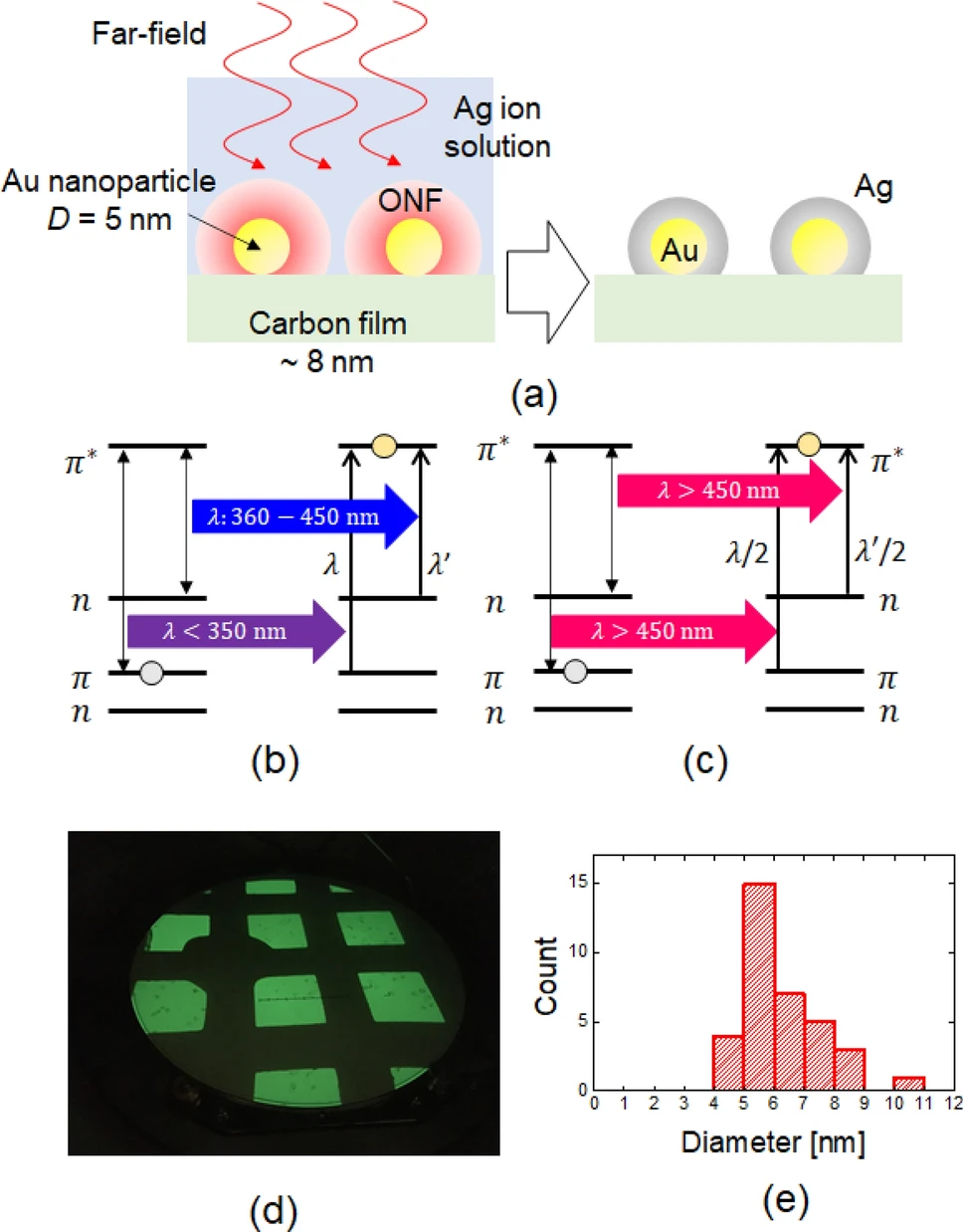
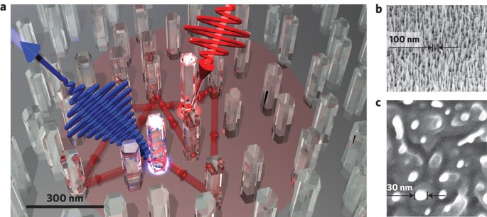
abstract = {By using gold (Au) nanoparticles (NPs) as an optical near-field source under far-field illumination in combination with a silver (Ag) ion solution containing a photoinitiator, we coated Ag on Au NPs using a near-field (NF)-assisted process. We evaluated the change in the size of the NPs using transmission electron microscopy. Evaluation of the synthesized Ag volume over illumination power confirmed the squared power dependence of the NP volume with illumination using 808 nm light, i.e., a wavelength longer than the absorption edge wavelength of the photoinitiator molecules. The rate of volume increase was much lower than the plasmonic field enhancement effect. Therefore, the squared power dependency of the volume increase using a wavelength longer than the absorption edge wavelength originated from NF-assisted second-harmonic generation and the resulting excitation.},
keywords = {First, Nanophotonic fabrication, Near-field effect, SHG},
pubstate = {published},
tppubtype = {article}
}
2020
Takashi Yatsui, Yuki Nakamura, Yosuke Suzuki, Tatsuki Morimoto, Yuma Kato, Muneaki Yamamoto, Tomoko Yoshida, Wataru Kurashige, Nobuyuki Shimizu, Yuichi Negishi, Kenji Iida, Katsuyuki Nobusada
Increase in CO2 reduction rate via optical near-field effect Journal Article
In: Journal of Nanophotonics, vol. 14, no. 4, pp. 046011, 2020.
Abstract | Links | BibTeX | タグ: CO2 reduction, Near-field effect
@article{CO2reduction,

title = {Increase in CO2 reduction rate via optical near-field effect},

author = {Takashi Yatsui and Yuki Nakamura and Yosuke Suzuki and Tatsuki Morimoto and Yuma Kato and Muneaki Yamamoto and Tomoko Yoshida and Wataru Kurashige and Nobuyuki Shimizu and Yuichi Negishi and Kenji Iida and Katsuyuki Nobusada},

doi = {10.1117/1.JNP.14.046011},

year  = {2020},

date = {2020-11-27},

journal = {Journal of Nanophotonics},

volume = {14},

number = {4},

pages = {046011},

abstract = {To reduce the effects of global warming, visible and near-infrared light must be used more efficiently. Deep ultraviolet light (8 eV) is required for the direct dissociation of CO2 by light; however, the introduction of a metal complex has made it possible to realize CO2 reduction with visible light. We demonstrate that the optical near field (ONF) can increase the CO2 reduction rate. For this, we used gold clusters, because they can be a suitable source for ONFs, as their size and density can be controlled by the number of gold atoms. By attaching a metal complex near gold clusters with diameters of 1.0 to 1.3 nm, we confirm that the reduction rate of CO2 to CO increased by 1.5 to 2.1 times. The gold clusters were sufficiently small; therefore, there was no plasmonic resonant peak or heat generation. Because the near-field effect is based on a photochemical reaction, it can be applied to other metal complexes used in CO2 reduction, and it has other applications such as water splitting and water purification.},

keywords = {CO2 reduction, Near-field effect},

pubstate = {published},

tppubtype = {article}

}

Chih-Zong Deng, Ya-Lun Ho, J. Kenji Clark, Takashi Yatsui, Jean-Jacques Delaunay
Light Switching with a Metal-Free Chiral-Sensitive Metasurface at Telecommunication Wavelengths Journal Article
In: ACS Photonics, vol. 7, no. 10, pp. 2915–2922, 2020.
Abstract | Links | BibTeX | タグ: Nanophotonic device, Near-field effect
@article{LightSwitching,

title = {Light Switching with a Metal-Free Chiral-Sensitive Metasurface at Telecommunication Wavelengths},

author = {Chih-Zong Deng and Ya-Lun Ho and J. Kenji Clark and Takashi Yatsui and Jean-Jacques Delaunay},

doi = {10.1021/acsphotonics.0c01377},

year  = {2020},

date = {2020-10-12},

urldate = {2020-10-12},

journal = {ACS Photonics},

volume = {7},

number = {10},

pages = {2915–2922},

abstract = {Controlling the direction of light propagation, or light switching, enables the addressing of individual optical elements in high-density and complex photonic integrated devices. Light switching is therefore crucial to the development of photonic/plasmonic integrated circuits. Chiral-sensitive metasurfaces using metallic nanostructures have been used to realize light switching by coupling incident light of different spins to surface plasmon polaritons propagating in different directions. However, surface plasmon polaritons-based devices suffer from short propagation lengths and narrow resonance wavelength ranges resulting from ohmic losses in their metal layers. Bloch surface waves can be seen as a metal-free analogy to surface plasmon polaritons with superior properties such as low propagation losses and wide operating wavelength ranges. Here, we demonstrate a metal-free chiral-sensitive Bloch-surface-wave switching circuit consisting of a carefully arranged array of U-shaped apertures, guiding slabs, and grating couplers. By engineering the amplitude and phase of the Bloch surface wave to achieve spin-controlled unidirectional coupling, control of the propagation direction of the Bloch surface waves is realized. Very high directional selectivity is reported at the telecommunications wavelength of 1550 nm, both theoretically at 23 dB and experimentally at 13.5 dB. The ability to realize spin-controlled light switching on a chip at telecommunications wavelengths using metal-free chiral-sensitive metasurfaces should benefit the development of low-loss on-chip photonic integrated devices.},

keywords = {Nanophotonic device, Near-field effect},

pubstate = {published},

tppubtype = {article}

}
2019
Naoya Tate, Takashi Yatsui
Visible light-induced thymine dimerisation based on large localised field gradient by non-uniform optical near-field Journal Article
In: Scientific Reports, vol. 9, pp. 18383, 2019.
Abstract | Links | BibTeX | タグ: DNA, Near-field effect, Non-uniform optical near field
@article{tate2019,
title = {Visible light-induced thymine dimerisation based on large localised field gradient by non-uniform optical near-field},
author = {Naoya Tate and Takashi Yatsui},
doi = {10.1038/s41598-019-54661-6},
year = {2019},
date = {2019-12-01},
journal = {Scientific Reports},
volume = {9},
pages = {18383},
publisher = {Springer Nature},
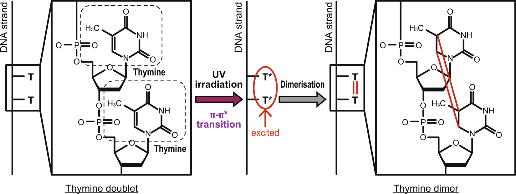
abstract = {The localised excitations of several molecular reactions utilising optical irradiation have been studied in the field of molecular physics. In particular, deoxyribonucleic acid (DNA) strands organise the genetic information of all living matter. Therefore, artificial methods for freely controlling reactions using only light irradiation are highly desirable for reactions of these strands; this in regard with artificial protein synthesis, regional genetic curing, and stochastic analysis of several genetic expressions. Generally, DNA strands have strong absorption features in the deep ultra-violet (DUV) region, which are related to the degradation and reconstruction of the strand bonding structures. However, irradiation by DUV light unavoidably induces unintended molecular reactions which can damage and break the DNA strands. In this paper, we report a photo-induced molecular reaction initiated by the irradiation of DNA strands with visible light. We utilised photo-dissociation from the vibrational levels induced by non-uniform optical near-fields surrounding nanometric Au particles to which DNA strands were attached. The results were experimentally observed by a reduction in the DUV absorbance of the DNA strands during irradiation. There was a much higher yield of molecular reactions than expected due to the absorbance of visible light, and no defects were caused in the DNA strands.},
keywords = {DNA, Near-field effect, Non-uniform optical near field},
pubstate = {published},
tppubtype = {article}
}
Takashi Yatsui
Recent improvement of silicon absorption in opto-electric devices Journal Article
In: Opto-Electronic Advances, vol. 2, no. 10, pp. 190023, 2019, (review article, selected as cover story).
Abstract | Links | BibTeX | タグ: Direct wave-vector excitation, First, First principle calculation, Indirect band gap, Near-field effect, Plasmon, Review, Si
@article{OEA_RefItem:1,

title = {Recent improvement of silicon absorption in opto-electric devices},

author = {Takashi Yatsui},

doi = {10.29026/oea.2019.190023},

year  = {2019},

date = {2019-10-01},

urldate = {2019-10-01},

journal = {Opto-Electronic Advances},

volume = {2},

number = {10},

pages = {190023},

publisher = {OEA},

abstract = {Silicon dominates the contemporary electronic industry. However, being an indirect band-gap material, it is a poor absorber of light, which decreases the efficiency of Si-based photodetectors and photovoltaic devices. This review highlights recent studies performed towards improving the optical absorption of Si. A summary of recent theoretical approaches based on the first principle calculation has been provided. It is followed by an overview of recent experimental approaches including scattering, plasmon, hot electron, and near-field effects. The article concludes with a perspective on the future research direction of Si-based photodetectors and photovoltaic devices.},

note = {review article, selected as cover story},

keywords = {Direct wave-vector excitation, First, First principle calculation, Indirect band gap, Near-field effect, Plasmon, Review, Si},

pubstate = {published},

tppubtype = {article}

}
Takashi Yatsui, Yusuke Nakahira, Yuki Nakamura, Tatsuki Morimoto, Yuma Kato, Muneaki Yamamoto, Tomoko Yoshida, Kenji Iida, Katsuyuki Nobusada
Realization of red shift of absorption spectra using optical near-field effect Journal Article
In: Nanotechnology, vol. 30, no. 34, pp. 34LT02, 2019.
Abstract | Links | BibTeX | タグ: CO2 reduction, First, Near-field effect
@article{Yatsui_2019,

title = {Realization of red shift of absorption spectra using optical near-field effect},

author = {Takashi Yatsui and Yusuke Nakahira and Yuki Nakamura and Tatsuki Morimoto and Yuma Kato and Muneaki Yamamoto and Tomoko Yoshida and Kenji Iida and Katsuyuki Nobusada},

doi = {10.1088/1361-6528/ab2092},

year  = {2019},

date = {2019-06-01},

journal = {Nanotechnology},

volume = {30},

number = {34},

pages = {34LT02},

publisher = {IOP Publishing},

abstract = {In many applications such as CO2 reduction and water splitting, high-energy photons in the ultraviolet region are required to complete the chemical reactions. However, to realize sustainable development, the photon energies utilized must be lower than the absorption edge of the materials including the metal complex for CO2 reduction, the electrodes for water splitting, because of the huge amount of lower energy than the visible region received from the sun. In the previous works, we had demonstrated that optical near-fields (ONFs) could realize chemical reactions, by utilizing photon energies much lower than the absorption edge because of the spatial non-uniformity of the electric field. In this paper, we demonstrate that an ONF can realize the red shift of the absorption spectra of the metal-complex material for photocatalytic reduction. By attaching the metal complex to ZnO nano-crystalline aggregates with nano-scale protrusions, the absorption spectra by using diffuse reflection of the metal complex can be shifted to a longer wavelength by 10.6 nm. The results of computational studies based on a first-principles computational program including the ONF effect provide proof of the increase in the absorption of the metal complex at lower photon energies. Since the near-field assisted field increase improves the carrier excitation in the metal-complex materials, this effect may be universal and it could applicable to CO2 reduction using the other metal-complex materials, as well as to the other photo excitation process including water splitting.},

keywords = {CO2 reduction, First, Near-field effect},

pubstate = {published},

tppubtype = {article}

}
2014
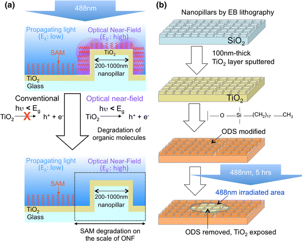
Hac Huong Thu Le, Kazuma Mawatari, Yuriy Pihosh, Tadashi Kawazoe, Takashi Yatsui, Motoichi Ohtsu, Takehiko Kitamori
Novel sub-100 nm surface chemical modification by optical near-field induced photocatalytic reaction Journal Article
In: Microfluidics and Nanofluidics, vol. 17, no. 4, pp. 751-758, 2014.
Abstract | Links | BibTeX | タグ: Nanophotonic fabrication, Near-field effect, Photocatalytic reaction
@article{2014Le,

title = {Novel sub-100 nm surface chemical modification by optical near-field induced photocatalytic reaction},

author = {Hac Huong Thu Le and Kazuma Mawatari and Yuriy Pihosh and Tadashi Kawazoe and Takashi Yatsui and Motoichi Ohtsu and Takehiko Kitamori},

doi = {10.1007/s10404-014-1361-7},

year  = {2014},

date = {2014-10-01},

journal = {Microfluidics and Nanofluidics},

volume = {17},

number = {4},

pages = {751-758},

publisher = {Springer Nature},

abstract = {The surface modification is indispensable to facilitate new functional applications of micro/nanofluidics devices. Among many modification techniques developed so far, the photo-induced chemical modification is the most versatile method in terms of robustness, process simplicity, and feasibility of chemical functionality. In particular, the method is useful for closed spaces, such as post-bonded devices. However, the limitation by optical diffraction limit is still a challenging issue in scaling down the pattern sizes to nanoscale. Here, we demonstrated a novel surface modification on sub-100 nm scale utilizing the novel optical near-field (ONF) generated on nanostructures of photocatalyst (TiO2). The minimum pattern size of 40 nm, which was much smaller than diffraction limit, was achieved using a visible light source (488 nm) and a conventional irradiation setup. The controllability of pattern size by light intensity, the feasibility of functionality, and the non-contact working mode have impacts on surface patterning of post-bonded micro/nanofluidics devices. It is also worthy to note that our results verified for the first time the ONF on nanostructures of non-metal materials and its ability to manipulate the chemical reaction on nanoscale.},

keywords = {Nanophotonic fabrication, Near-field effect, Photocatalytic reaction},

pubstate = {published},

tppubtype = {article}

}

Wataru Nomura, Makoto Naruse, Masashi Aono, Song-Ju Kim, Tadashi Kawazoe, Takashi Yatsui, Motoichi Ohtsu
In: Advances in Optical Technologies, vol. 2014, pp. 569684, 2014.
Abstract | Links | BibTeX | タグ: Nanophotonic device, Near-field effect, QD
@article{2014NomuraY,

title = {Demonstration of Controlling the Spatiotemporal Dynamics of Optical Near-Field Excitation Transfer in Y-Junction Structure Consisting of Randomly Distributed Quantum Dots},

author = {Wataru Nomura and Makoto Naruse and Masashi Aono and Song-Ju Kim and Tadashi Kawazoe and Takashi Yatsui and Motoichi Ohtsu},

doi = {10.1155/2014/569684},

year  = {2014},

date = {2014-02-01},

urldate = {2014-02-01},

journal = {Advances in Optical Technologies},

volume = {2014},

pages = {569684},

abstract = {Solution searching devices that operate on the basis of controlling the spatiotemporal dynamics of excitation transfer via dressed photon interactions between quantum dots have been proposed. Long-range excitation transfer based on dressed photon interactions between randomly distributed quantum dots is considered to be effective in realizing such devices. Here, we successfully controlled the spatiotemporal dynamics of excitation transfer using a Y-junction structure consisting of randomly dispersed CdSe/ZnS core-shell quantum dots. This Y-junction structure has two “output ends” and one “tap end.” By exciting one output end with control light, we observed increased excitation transfer to the other output end via a state-filling effect. Conversely, we observed reduced excitation transfer to the output ends by irradiating the tap end with control light, due to excitation of defect levels in the tap end. These results show the possibility of controlling the optical excitation transfer dynamics between multiple quantum dots.},

keywords = {Nanophotonic device, Near-field effect, QD},

pubstate = {published},

tppubtype = {article}

}
2013
Naoya Tate, Makoto Naruse, Yang Liu, Tadashi Kawazoe, Takashi Yatsui, Motoichi Ohtsu
Experimental demonstration and stochastic modeling of autonomous formation of nanophotonic droplets Journal Article
In: Applied Physics B, vol. 112, no. 4, pp. 587-592, 2013.
Abstract | Links | BibTeX | タグ: Droplet, Nanophotonic fabrication, Near-field effect
@article{2013tateAPB3,

title = {Experimental demonstration and stochastic modeling of autonomous formation of nanophotonic droplets},

author = {Naoya Tate and Makoto Naruse and Yang Liu and Tadashi Kawazoe and Takashi Yatsui and Motoichi Ohtsu},

doi = {10.1007/s00340-013-5442-1},

year  = {2013},

date = {2013-09-01},

journal = {Applied Physics B},

volume = {112},

number = {4},

pages = {587-592},

publisher = {Springer Nature},

abstract = {We have previously demonstrated a novel technique for autonomously forming a nanophotonic droplet, which is micro-scale spherical polymer structure that contains paired heterogeneous nanometric components. The sort-selectivity and alignment accuracy of the nanometric components in each nanophotonic droplet, and the related homogeneity of the optical function, are due to a characteristic pairing process based on a phonon-assisted photo-curing method. The proposed method requires irradiating a mixture of components with light to induce optical near-field interactions between each component, and subsequent processes based on these interactions. The pairing yield of components via the interactions is considered to mainly depend on the frequency of their encounters and the size-resonance effect between encountered components. In this paper, we model these two factors by individual stochastic procedures and construct a numerical model to describe the pairing process. Agreement between the results of numerical and experimental demonstrations shows the validity of our stochastic modeling.},

keywords = {Droplet, Nanophotonic fabrication, Near-field effect},

pubstate = {published},

tppubtype = {article}

}
2012

Pham Nam Hai, Wataru Nomura, Takashi Yatsui, Motoichi Ohtsu, Masaaki Tanaka
Effects of laser irradiation on the self-assembly of MnAs nanoparticles in a GaAs matrix Journal Article
In: Applied Physics Letters, vol. 101, no. 19, pp. 193102, 2012.
Abstract | Links | BibTeX | タグ: Nanoparticle, Nanophotonic fabrication, Near-field effect
@article{doi:10.1063/1.4765355,

title = {Effects of laser irradiation on the self-assembly of MnAs nanoparticles in a GaAs matrix},

author = {Pham Nam Hai and Wataru Nomura and Takashi Yatsui and Motoichi Ohtsu and Masaaki Tanaka},

doi = {10.1063/1.4765355},

year  = {2012},

date = {2012-10-01},

urldate = {2012-10-01},

journal = {Applied Physics Letters},

volume = {101},

number = {19},

pages = {193102},

abstract = {We investigate the effects of laser irradiation on the self-assembly of MnAs nanoparticles during solid-phase decomposition in a GaAs matrix. It is found that laser irradiation suppresses the growth of MnAs nanoparticles from small to large size, and that the median diameter D1 in the size distribution of small MnAs nanoparticles depends on the incident photon energy E following D1 ∼ E−1/5. We explain this behavior by the desorption of Mn atoms on the MnAs nanoparticle surface due to resonant optical absorption, in which incident photons excite intersubband electronic transitions between the quantized energy levels in the MnAs nanoparticles.},

keywords = {Nanoparticle, Nanophotonic fabrication, Near-field effect},

pubstate = {published},

tppubtype = {article}

}
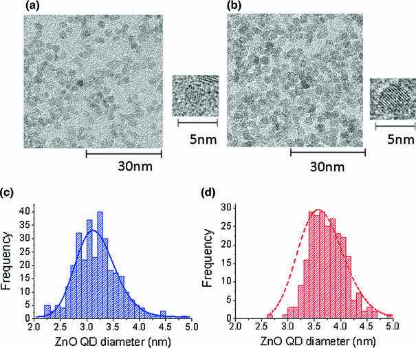
Yang Liu, Takashi Yatsui, Motoichi Ohtsu
Controlling the sizes of ZnO quantum dots by using dressed photon-phonon assisted sol-gel method Journal Article
In: Applied Physics B, vol. 108, no. 4, pp. 707-711, 2012.
Abstract | Links | BibTeX | タグ: Nanophotonic fabrication, Near-field effect, QD, Sol-gel, ZnO
@article{2012liuAPB,

title = {Controlling the sizes of ZnO quantum dots by using dressed photon-phonon assisted sol-gel method},

author = {Yang Liu and Takashi Yatsui and Motoichi Ohtsu},

doi = {10.1007/s00340-012-5151-1},

year  = {2012},

date = {2012-09-01},

journal = {Applied Physics B},

volume = {108},

number = {4},

pages = {707-711},

publisher = {Springer Nature},

abstract = {We developed a sol-gel method using the dressed photon-phonon (DPP) process. DPPs are selectively exited in nanoscale structures at photon energies that are lower than the bandgap energy, which allows one to increase the growth rate of smaller ZnO quantum dots (QDs). Thus, we obtained a smaller size variance of ZnO QDs. The growth rate was proportional to the power of the light used for DPP excitation. The results were confirmed using a rate equation that accounted for the concentration of the sol-gel solution.},

keywords = {Nanophotonic fabrication, Near-field effect, QD, Sol-gel, ZnO},

pubstate = {published},

tppubtype = {article}

}
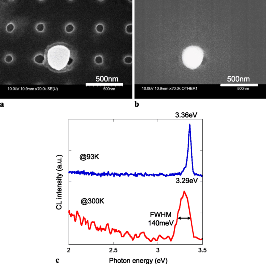
Takashi Yatsui, Kosuke Nakanishi, Kokoro Kitamura, Motoichi Ohtsu
Room-temperature growth of high-quality ZnO nanocrystals using a dressed-photon-assisted near-field process Journal Article
In: Applied Physics B, vol. 107, no. 3, pp. 637-641, 2012.
Abstract | Links | BibTeX | タグ: First, Near-field effect, ZnO
@article{2012yatsuiAPB,

title = {Room-temperature growth of high-quality ZnO nanocrystals using a dressed-photon-assisted near-field process},

author = {Takashi Yatsui and Kosuke Nakanishi and Kokoro Kitamura and Motoichi Ohtsu},

doi = {10.1007/s00340-012-5076-8},

year  = {2012},

date = {2012-05-01},

journal = {Applied Physics B},

volume = {107},

number = {3},

pages = {637-641},

publisher = {Springer Nature},

abstract = {Single-crystalline ZnO nanocrystals were fabricated by room-temperature photo-chemical vapor deposition (PCVD). We further enhanced the growth of high-quality single-crystalline ZnO nanocrystals using dressed photons and phonons (DPPs). This resulted in greater position control and the growth of high-quality ZnO nanocrystals. The ZnO nanocrystals produced with DPPs had excellent cathodoluminescence characteristics, indicating that the near-field PCVD process could be a promising technique for nanophotonic integrated circuit production.},

keywords = {First, Near-field effect, ZnO},

pubstate = {published},

tppubtype = {article}

}

Takashi Yatsui, Masahiro Tsuji, Yang Liu, Tadashi Kawazoe, Motoichi Ohtsu
Emission from a dipole-forbidden energy state in a ZnO quantum dot induced by a near-field interaction with a fiber probe Journal Article
In: Applied Physics Letters, vol. 100, no. 22, pp. 223110, 2012.
Abstract | Links | BibTeX | タグ: First, Near-field effect, QD, ZnO
@article{doi:10.1063/1.4723574,

title = {Emission from a dipole-forbidden energy state in a ZnO quantum dot induced by a near-field interaction with a fiber probe},

author = {Takashi Yatsui and Masahiro Tsuji and Yang Liu and Tadashi Kawazoe and Motoichi Ohtsu},

doi = {10.1063/1.4723574},

year  = {2012},

date = {2012-05-01},

urldate = {2012-05-01},

journal = {Applied Physics Letters},

volume = {100},

number = {22},

pages = {223110},

abstract = {The emission intensity from the dipole-forbidden state in a spherical quantum dot (QD) was enhanced by introducing an aperture fiber probe close to the ZnO QD to induce a near-field interaction between the probe tip and the QD. The cross-sectional profiles of the photoluminescence intensities of the ground exciton state and the excited exciton states varied spatially in an anti-correlated manner.},

keywords = {First, Near-field effect, QD, ZnO},

pubstate = {published},

tppubtype = {article}

}
Manfred Mascheck, Stephen Schmidt, Martin Silies, Takashi Yatsui, Kokoro Kitamura, Motoichi Ohtsu, David Leipold, Erich Runge, Christoph Lienau
Observing the localization of light in space and time by ultrafast second-harmonic microscopy Journal Article
In: Nature Photonics, vol. 6, no. 5, pp. 293-298, 2012.
Abstract | Links | BibTeX | タグ: Near-field effect, Selected, SHG
@article{2012NatPhoton,

title = {Observing the localization of light in space and time by ultrafast second-harmonic microscopy},

author = {Manfred Mascheck and Stephen Schmidt and Martin Silies and Takashi Yatsui and Kokoro Kitamura and Motoichi Ohtsu and David Leipold and Erich Runge and Christoph Lienau},

url = {https://www.altmetric.com/details/698801},

doi = {10.1038/nphoton.2012.69},

year  = {2012},

date = {2012-05-01},

journal = {Nature Photonics},

volume = {6},

number = {5},

pages = {293-298},

publisher = {Springer Nature},

abstract = {Multiple coherent scattering and the constructive interference of certain scattering paths form the common scheme of several remarkable localization phenomena of classical and quantum waves in randomly disordered media. Prominent examples are electron transport in disordered conductors, the localization of excitons in semiconductor nanostructures, surface plasmon polaritons at rough metallic films or light in disordered dielectrics and amplifying media. However, direct observation of the fundamental spatiotemporal dynamics of the localization process remains challenging. This holds true, in particular, for the localization of light occurring on exceedingly short femtosecond timescales and nanometre length scales. Here, we combine second harmonic microscopy with few-cycle time resolution to probe the spatiotemporal localization of light waves in a random dielectric medium. We find lifetimes of the photon modes of several femtoseconds and a broad distribution of the local optical density of states, revealing central hallmarks of the localization of light.},

keywords = {Near-field effect, Selected, SHG},

pubstate = {published},

tppubtype = {article}

}

Makoto Naruse, Yang Liu, Wataru Nomura, Takashi Yatsui, Masaki Aida, Laszlo B Kish, Motoichi Ohtsu
Stochastic processes in light-assisted nanoparticle formation Journal Article
In: Applied Physics Letters, vol. 100, no. 19, pp. 193106, 2012.
Abstract | Links | BibTeX | タグ: Near-field effect
@article{doi:10.1063/1.4711808,

title = {Stochastic processes in light-assisted nanoparticle formation},

author = {Makoto Naruse and Yang Liu and Wataru Nomura and Takashi Yatsui and Masaki Aida and Laszlo B Kish and Motoichi Ohtsu},

doi = {10.1063/1.4711808},

year  = {2012},

date = {2012-04-01},

urldate = {2012-04-01},

journal = {Applied Physics Letters},

volume = {100},

number = {19},

pages = {193106},

abstract = {Recently, light-assisted nanofabrication have been introduced, such as the synthesis of quantum dots using photo-induced desorption that yields reduced size fluctuations or metal sputtering under light illumination resulting in self-organized, nanoparticle chains. The physical mechanisms have originally been attributed to material desorption or plasmon resonance effects. However, significant stochastic phenomena are also present that have not been explained yet. We introduce stochastic models taking account of the light-assisted processes that reproduce phenomenological characteristics consistent with the experimental observations.},

keywords = {Near-field effect},

pubstate = {published},

tppubtype = {article}

}
Wataru Nomura, Takashi Yatsui, Tadashi Kawazoe, Makoto Naruse, Erich Runge, Christoph Lienau, Motoichi Ohtsu
Direct observation of optical excitation transfer based on resonant optical near-field interaction Journal Article
In: Applied Physics B, vol. 107, no. 2, pp. 257-262, 2012.
Abstract | Links | BibTeX | タグ: Nanophotonic device, Near-field effect, QD
@article{2012nomuraAPB,
title = {Direct observation of optical excitation transfer based on resonant optical near-field interaction},
author = {Wataru Nomura and Takashi Yatsui and Tadashi Kawazoe and Makoto Naruse and Erich Runge and Christoph Lienau and Motoichi Ohtsu},
doi = {10.1007/s00340-012-5009-6},
year = {2012},
date = {2012-04-01},
journal = {Applied Physics B},
volume = {107},
number = {2},
pages = {257-262},
publisher = {Springer Nature},
abstract = {This article reports the direct observation of long-distance optical excitation transfer based on resonant optical near-field interactions in randomly distributed quantum dots (QDs). We fabricated optical excitation transfer paths based on randomly distributed QDs by using CdSe/ZnS core-shell QDs and succeeded for the first time in obtaining output signals resulting from a unidirectional optical excitation transfer length of 2.4 Êm. Furthermore, we demonstrate that the optical excitation transfer occurs via the resonant excited levels of the QDs with a comparative experiment using non-resonant QDs. This excitation-transfer mechanism allows for intersecting, non-interacting nano-optical wires.},
keywords = {Nanophotonic device, Near-field effect, QD},
pubstate = {published},
tppubtype = {article}
}
2011

Thu Hac Huong Le, Kazuma Mawatari, Yuriy Pihosh, Tadashi Kawazoe, Takashi Yatsui, Motoichi Ohtsu, Masahiro Tosa, Takehiko Kitamori
Optical near-field induced visible response photoelectrochemical water splitting on nanorod TiO2 Journal Article
In: Applied Physics Letters, vol. 99, no. 21, pp. 213105, 2011.
Abstract | Links | BibTeX | タグ: nanorod, Near-field effect, TiO2, Water splitting
@article{doi:10.1063/1.3663632,

title = {Optical near-field induced visible response photoelectrochemical water splitting on nanorod TiO2},

author = {Thu Hac Huong Le and Kazuma Mawatari and Yuriy Pihosh and Tadashi Kawazoe and Takashi Yatsui and Motoichi Ohtsu and Masahiro Tosa and Takehiko Kitamori},

url = {https://doi.org/10.1063/1.3663632},

doi = {10.1063/1.3663632},

year  = {2011},

date = {2011-11-01},

urldate = {2011-11-01},

journal = {Applied Physics Letters},

volume = {99},

number = {21},

pages = {213105},

abstract = {Here we report a way to induce the visible response of non-doped TiO2 in the photocatalytic electrochemical water splitting, which is achieved by utilizing the optical near-field (ONF) generated on nanorod TiO2. The visible response is attributed to the ONF-induced phonon-assisted excitation process, in which TiO2 is excited by sub-bandgap photons via phonon energy. Our approach directly gets involved in the excitation process without chemical modification of materials; accordingly it is expected to have few drawbacks on the photocatalytic performance. This study may offer another perspective on the development of solar harvesting materials.},

keywords = {nanorod, Near-field effect, TiO2, Water splitting},

pubstate = {published},

tppubtype = {article}

}
Makoto Naruse, Tadashi Kawazoe, Takashi Yatsui, Naoya Tate, Motoichi Ohtsu
A stochastic modeling of morphology formation by optical near-field processes Journal Article
In: Applied Physics B, vol. 105, no. 4, pp. 185-190, 2011.
Abstract | Links | BibTeX | タグ: Near-field effect
@article{2011noruseAPB,

title = {A stochastic modeling of morphology formation by optical near-field processes},

author = {Makoto Naruse and Tadashi Kawazoe and Takashi Yatsui and Naoya Tate and Motoichi Ohtsu},

doi = {10.1007/s00340-011-4708-8},

year  = {2011},

date = {2011-11-01},

journal = {Applied Physics B},

volume = {105},

number = {4},

pages = {185-190},

publisher = {Springer Nature},

abstract = {We previously reported (S. Yukutake et al. in Appl. Phys. B 99:415, 2010) that by depositing Ag particles on the electrode of a photovoltaic device composed of poly(3-hexylthiophene) (P3HT) and ZnO under light illumination (wavelength 660 nm) while reversely biasing the P3HT/ZnO p-n junction, a unique granular Ag film was formed. The resultant device generated a photocurrent at wavelengths as long as 670 nm, which is longer than the long-wavelength cutoff (=570 nm) of P3HT. Such an effect originates from a phonon-assisted process induced by an optical near field. In this paper, we analyze the morphological character of the Ag clusters and build a stochastic model in order to understand the principles behind the self-organized pattern formation process. The modeling includes the geometrical character of the material, its associated optical near fields, and the materials that flow in and out of the system. The model demonstrates behavior consistent with that observed in the experiment. We can see these phenomena as a new kind of self-organized criticality taking account of near-field effects, which will provide an insight into the analysis and design of future nanophotonic devices.},

keywords = {Near-field effect},

pubstate = {published},

tppubtype = {article}

}
Naoya Tate, Makoto Naruse, Wataru Nomura, Tadashi Kawazoe, Takashi Yatsui, Morihisa Hoga, Yasuyuki Ohyagi, Yoko Sekine, Hiroshi Fujita, Motoichi Ohtsu
Demonstration of modulatable optical near-field interactions between dispersed resonant quantum dots Journal Article
In: Optics Express, vol. 19, no. 19, pp. 18260-18271, 2011.
Abstract | Links | BibTeX | タグ: Near-field effect, QD
@article{Tate:11,

title = {Demonstration of modulatable optical near-field interactions between dispersed resonant quantum dots},

author = {Naoya Tate and Makoto Naruse and Wataru Nomura and Tadashi Kawazoe and Takashi Yatsui and Morihisa Hoga and Yasuyuki Ohyagi and Yoko Sekine and Hiroshi Fujita and Motoichi Ohtsu},

doi = {10.1364/OE.19.018260},

year  = {2011},

date = {2011-09-12},

journal = {Optics Express},

volume = {19},

number = {19},

pages = {18260-18271},

publisher = {OSA},

abstract = {We experimentally demonstrated the basic concept of modulatable optical near-field interactions by utilizing energy transfer between closely positioned resonant CdSe/ZnS quantum dot (QD) pairs dispersed on a flexible substrate. Modulation by physical flexion of the substrate changes the distances between quantum dots to control the magnitude of the coupling strength. The modulation capability was qualitatively confirmed as a change of the emission spectrum. We defined two kinds of modulatability for quantitative evaluation of the capability, and an evident difference was revealed between resonant and non-resonant QDs.},

keywords = {Near-field effect, QD},

pubstate = {published},

tppubtype = {article}

}
2010
Kokoro Kitamura, Takashi Yatsui, Tadashi Kawazoe, Masakazu Sugiyama, Motoichi Ohtsu
Site-selective deposition of gold nanoparticles using non-adiabatic reaction induced by optical near-fields Journal Article
In: Nanotechnology, vol. 21, no. 28, pp. 285302, 2010.
Abstract | Links | BibTeX | タグ: Nanophotonic fabrication, nanorod, Near-field effect, ZnO
@article{Kitamura_2010,

title = {Site-selective deposition of gold nanoparticles using non-adiabatic reaction induced by optical near-fields},

author = {Kokoro Kitamura and Takashi Yatsui and Tadashi Kawazoe and Masakazu Sugiyama and Motoichi Ohtsu},

doi = {10.1088/0957-4484/21/28/285302},

year  = {2010},

date = {2010-06-01},

journal = {Nanotechnology},

volume = {21},

number = {28},

pages = {285302},

publisher = {IOP Publishing},

abstract = {In this paper, we report on site-selective deposition of metal nanoparticles

using a non-adiabatic photochemical reaction. Photoreduction of gold

was performed in a silica gel membrane containing tetrachloroaurate (AuCl4 − ) ions, using ZnO nanorods as the sources of optical near-field light, resulting in deposition

of gold nanoparticles with an average diameter of 17.7 nm. The distribution of

distances between the gold nanoparticles and nanorod traces revealed that the gold

nanoparticles were deposited adjacent to the ZnO nanorods, reflecting the attenuation of

the optical near-fields in the vicinity of the ZnO nanorods. We found that the

emission wavelength from the ZnO nanorods was longer than the absorption edge

wavelength of the tetrachloroaurate. Additionally, from the intensity distribution

obtained by a finite-difference time-domain method, the gold deposited around the

ZnO nanorods was found to be due to a non-adiabatic photochemical reaction.},

keywords = {Nanophotonic fabrication, nanorod, Near-field effect, ZnO},

pubstate = {published},

tppubtype = {article}

}
using a non-adiabatic photochemical reaction. Photoreduction of gold
was performed in a silica gel membrane containing tetrachloroaurate (AuCl4 − ) ions, using ZnO nanorods as the sources of optical near-field light, resulting in deposition
of gold nanoparticles with an average diameter of 17.7 nm. The distribution of
distances between the gold nanoparticles and nanorod traces revealed that the gold
nanoparticles were deposited adjacent to the ZnO nanorods, reflecting the attenuation of
the optical near-fields in the vicinity of the ZnO nanorods. We found that the
emission wavelength from the ZnO nanorods was longer than the absorption edge
wavelength of the tetrachloroaurate. Additionally, from the intensity distribution
obtained by a finite-difference time-domain method, the gold deposited around the
ZnO nanorods was found to be due to a non-adiabatic photochemical reaction.
Sotaro Yukutake, Tadashi Kawazoe, Takashi Yatsui, Wataru Nomura, Kokoro Kitamura, Motoichi Ohtsu
In: Applied Physics B, vol. 99, no. 3, pp. 415-422, 2010.
Abstract | Links | BibTeX | タグ: Nanophotonic fabrication, Near-field effect, Self-assembly
@article{2010yukutakeAPB,

title = {Selective photocurrent generation in the transparent wavelength range of a semiconductor photovoltaic device using a phonon-assisted optical near-field process},

author = {Sotaro Yukutake and Tadashi Kawazoe and Takashi Yatsui and Wataru Nomura and Kokoro Kitamura and Motoichi Ohtsu},

doi = {10.1007/s00340-010-3999-5},

year  = {2010},

date = {2010-05-01},

journal = {Applied Physics B},

volume = {99},

number = {3},

pages = {415-422},

publisher = {Springer Nature},

abstract = {In this paper, we propose a novel photovoltaic device using P3HT and ZnO as test materials for the ptype and n-type semiconductors, respectively. To fabricate an electrode of this device, Ag was deposited on a P3HT film by RF-sputtering under light illumination (wavelength λ0 = 660 nm) while reversely biasing the P3HT/ZnO pnjunction. As a result, a unique granular Ag film was formed, which originated from a phonon-assisted process induced by an optical near-field in a self-organized manner. The fabricated device generated a photocurrent even though the incident light wavelength was as long as 670 nm, which is longer than the long-wavelength cutoff λc (= 570 nm) of the P3HT. The photocurrent was generated in a wavelength-selective manner, showing a maximum at the incident light wavelength of 620 nm, which was shorter than λ0 because of the Stark effect brought about by the reverse bias DC electric field applied during the Ag deposition.},

keywords = {Nanophotonic fabrication, Near-field effect, Self-assembly},

pubstate = {published},

tppubtype = {article}

}
Wataru Nomura, Takashi Yatsui, Yoshihata Yanase, Kenji Suzuki, Mitsuhiro Fujita, Atsushi Kamata, Makoto Naruse, Motoichi Ohtsu
Repairing nanoscale scratched grooves on polycrystalline ceramics using optical near-field assisted sputtering Journal Article
In: Applied Physics B, vol. 99, no. 1-2, pp. 75-78, 2010.
Abstract | Links | BibTeX | タグ: Nanophotonic fabrication, Near-field effect
@article{2010nomuraAPBrepair,

title = {Repairing nanoscale scratched grooves on polycrystalline ceramics using optical near-field assisted sputtering},

author = {Wataru Nomura and Takashi Yatsui and Yoshihata Yanase and Kenji Suzuki and Mitsuhiro Fujita and Atsushi Kamata and Makoto Naruse and Motoichi Ohtsu},

doi = {10.1007/s00340-009-3797-0},

year  = {2010},

date = {2010-04-01},

journal = {Applied Physics B},

volume = {99},

number = {1-2},

pages = {75-78},

publisher = {Springer Nature},

abstract = {We propose an optical near-field assisted sputtering method for repairing scratches on the surface of polycrystalline ceramics in a self-assembling manner. An Al2O3 source was sputtered on substrates with laser radiation of wavelength 473 nm. The average depth of the scratched grooves on polycrystalline Al2O3 ceramic substrate decreased from 3.2 nm to 0.79 nm. Using a Hough transform, we also confirmed the selective repair of scratches.},

keywords = {Nanophotonic fabrication, Near-field effect},

pubstate = {published},

tppubtype = {article}

}
Naoya Tate, Hiroki Tokoro, Keiji Takeda, Wataru Nomura, Takashi Yatsui, Tadashi Kawazoe, Makoto Naruse, Shin-ichi Ohkoshi, Motoichi Ohtsu
Transcription of optical near-fields by photoinduced structural change in single crystal metal complexes for parallel nanophotonic processing Journal Article
In: Applied Physics B, vol. 98, no. 4, pp. 685-689, 2010.
Abstract | Links | BibTeX | タグ: Nanophotonic fabrication, Near-field effect
@article{2010tateAPB,

title = {Transcription of optical near-fields by photoinduced structural change in single crystal metal complexes for parallel nanophotonic processing},

author = {Naoya Tate and Hiroki Tokoro and Keiji Takeda and Wataru Nomura and Takashi Yatsui and Tadashi Kawazoe and Makoto Naruse and Shin-ichi Ohkoshi and Motoichi Ohtsu},

doi = {10.1007/s00340-009-3772-9},

year  = {2010},

date = {2010-03-01},

journal = {Applied Physics B},

volume = {98},

number = {4},

pages = {685-689},

publisher = {Springer Nature},

abstract = {Exploiting the unique attributes of nanometer-scaled optical near-field interactions in a completely parallel manner is important for nanophotonics for enhancing the throughput in obtaining two-dimensional information on the nanometer scale, as well as for developing more practical and easy characterization or utilization of optical near-fields. In this paper, we propose transcription of optical near-fields, whereby their effects are spatially magnified so as to be detected in optical far fields. By utilizing cyano-bridged metal complexes that exhibit photoinduced structural changes, transcription at the nanometric scale can be realized. We synthesized single crystals of such metal complexes and observed their photoinduced phase changes. We experimentally achieved photoinduced structural changes via optical near-fields, which is the fundamental process in their transcription.},

keywords = {Nanophotonic fabrication, Near-field effect},

pubstate = {published},

tppubtype = {article}

}
Naoya Tate, Wataru Nomura, Takashi Yatsui, Tadashi Kawazoe, Makoto Naruse, Motoichi Ohtsu
Parallel Retrieval of Nanometer-Scale Light-Matter Interactions for Nanophotonic Systems Journal Article
In: Natural Computing , pp. 298-307, 2010, ISBN: 978-4-431-53868-4.
Abstract | Links | BibTeX | タグ: Near-field effect
@article{10.1007/978-4-431-53868-4_34,

title = {Parallel Retrieval of Nanometer-Scale Light-Matter Interactions for Nanophotonic Systems},

author = {Naoya Tate and Wataru Nomura and Takashi Yatsui and Tadashi Kawazoe and Makoto Naruse and Motoichi Ohtsu},

doi = {10.1007/978-4-431-53868-4_34},

isbn = {978-4-431-53868-4},

year  = {2010},

date = {2010-01-01},

booktitle = {Natural Computing},

journal = {Natural Computing },

pages = {298-307},

publisher = {Springer Japan},

address = {Tokyo},

abstract = {Exploiting the unique attributes of nanometer-scale optical near-field interactions in a completely parallel manner is important for innovative nanometric optical processing systems. In this paper, we propose the basic concepts necessary for parallel retrieval of light--matter interactions on the nanometer-scale instead of the conventional one-dimensional scanning method. One is the macro-scale observation of optical near-fields, and the other is the transcription of optical near-fields. The former converts effects occurring locally on the nanometer scale involving optical near-field interactions to propagating light radiation, and the latter magnifies the distributions of optical near-fields from the nanometer scale to the sub-micrometer one. Those techniques allow us to observe optical far-field signals that originate from the effects occurring at the nanometer scale. We numerically verified the concepts and principles using electromagnetic simulations.},

keywords = {Near-field effect},

pubstate = {published},

tppubtype = {article}

}
2009
Takashi Yatsui, Shunsuke Yamazaki, Keiichi Ito, Hiroshi Kawamura, Michinobu Mizumura, Tadashi Kawazoe, Motoichi Ohtsu
Increased spatial homogeneity in a light-emitting InGaN thin film using optical near-field desorption Journal Article
In: Applied Physics B, vol. 97, no. 2, pp. 375-378, 2009.
Abstract | Links | BibTeX | タグ: First, GaN, Nanophotonic fabrication, Near-field effect, Self-assembly
@article{2009yatsuiGaNAPB,

title = {Increased spatial homogeneity in a light-emitting InGaN thin film using optical near-field desorption},

author = {Takashi Yatsui and Shunsuke Yamazaki and Keiichi Ito and Hiroshi Kawamura and Michinobu Mizumura and Tadashi Kawazoe and Motoichi Ohtsu},

doi = {10.1007/s00340-009-3757-8},

year  = {2009},

date = {2009-10-01},

journal = {Applied Physics B},

volume = {97},

number = {2},

pages = {375-378},

publisher = {Springer Nature},

abstract = {We report a self-assembly method that produces greater spatial uniformity in InGaN thin films using optical near-field desorption. Spatial homogeneity in the In fraction was reduced by introducing additional light during the photo-enhanced chemical vapor deposition of InGaN. Near-field desorption of InGaN nanoparticles, upon addition depended on the In content of the film, and the photon energy of the illumination source determined the energy of the emitted photons. Since this deposition method is based on a photo-desorption reaction, it can easily be applied to other deposition techniques and used with other semiconductor systems.},

keywords = {First, GaN, Nanophotonic fabrication, Near-field effect, Self-assembly},

pubstate = {published},

tppubtype = {article}

}

Takashi Yatsui, Motoichi Ohtsu
Production of size-controlled Si nanocrystals using self-organized optical near-field chemical etching Journal Article
In: Applied Physics Letters, vol. 95, no. 4, pp. 043104, 2009.
Abstract | Links | BibTeX | タグ: First, Nanophotonic fabrication, Near-field effect, Self-assembly, Si
@article{doi:10.1063/1.3193536,

title = {Production of size-controlled Si nanocrystals using self-organized optical near-field chemical etching},

author = {Takashi Yatsui and Motoichi Ohtsu},

doi = {10.1063/1.3193536},

year  = {2009},

date = {2009-07-24},

urldate = {2009-07-24},

journal = {Applied Physics Letters},

volume = {95},

number = {4},

pages = {043104},

abstract = {We demonstrate the selective photochemical etching of Si in a self-organized manner, which strongly depends on the distribution of the optical near field. This dependence was described by the virtual exciton-phonon-polariton model. The photoluminescence (PL) spectra from the etched Si exhibited a blueshifted PL peak at 1.8 eV, corresponding to Si nanocrystals of 2.8 nm diameter.},

keywords = {First, Nanophotonic fabrication, Near-field effect, Self-assembly, Si},

pubstate = {published},

tppubtype = {article}

}
Kiyoshi Kobayashi, Arata Sato, Takashi Yatsui, Tadashi Kawazoe, Motoichi Ohtsu
New Aspects in Nanofabrication Using Near-Field Photo-Chemical Vapor Deposition Journal Article
In: Applied Physics Express, vol. 2, no. 7, pp. 075504, 2009.
Abstract | Links | BibTeX | タグ: Nanophotonic fabrication, Near-field effect
@article{Kobayashi_2009,

title = {New Aspects in Nanofabrication Using Near-Field Photo-Chemical Vapor Deposition},

author = {Kiyoshi Kobayashi and Arata Sato and Takashi Yatsui and Tadashi Kawazoe and Motoichi Ohtsu},

doi = {10.1143/apex.2.075504},

year  = {2009},

date = {2009-07-01},

journal = {Applied Physics Express},

volume = {2},

number = {7},

pages = {075504},

publisher = {IOP Publishing},

abstract = {On the basis of the dressing nature of optical near fields and the important role of optically forbidden molecular vibrational excitations, a simple model is proposed to describe atom or atom cluster desorption due to optical near fields from a nanodot deposited on a substrate. Assuming an anharmonic potential for each atomic binding, we evaluate an effective atom–nanodot potential to determine the desorption energy and stabilized dot size. The model describes the reported experimental data reasonably well, and shows that optically forbidden molecular vibrational excitations play an important role in optical near-field processes, which could potentially leads to a new fabrication method in addition to the controlling the size and position of nanostructures.},

keywords = {Nanophotonic fabrication, Near-field effect},

pubstate = {published},

tppubtype = {article}

}
Naoya Tate, Wataru Nomura, Takashi Yatsui, Makoto Naruse, Motoichi Ohtsu
Hierarchy in optical near-fields based on compositions of nanomaterials Journal Article
In: Applied Physics B, vol. 96, no. 1, pp. 1-4, 2009.
Abstract | Links | BibTeX | タグ: Near-field effect
@article{2009tateAPB,

title = {Hierarchy in optical near-fields based on compositions of nanomaterials},

author = {Naoya Tate and Wataru Nomura and Takashi Yatsui and Makoto Naruse and Motoichi Ohtsu},

doi = {10.1007/s00340-008-3354-2},

year  = {2009},

date = {2009-07-01},

journal = {Applied Physics B},

volume = {96},

number = {1},

pages = {1-4},

publisher = {Springer Nature},

abstract = {Optical near-field interactions exhibit hierarchical responses in the nanometer scale allowing unique functions in nanophotonic systems. Such hierarchical properties in optical near-fields originate various physical entities in the nanometer scale. Engineering nanomaterial compositions, while maintaining geometrically equivalent conditions, leads to characteristic hierarchical responses. We experimentally demonstrate such material-dependent optical near-field hierarchy using core-shell-type nanostructures composed of gold and silver.},

keywords = {Near-field effect},

pubstate = {published},

tppubtype = {article}

}
Naoya Tate, Hiroki Sugiyama, Makoto Naruse, Wataru Nomura, Takashi Yatsui, Tadashi Kawazoe, Motoichi Ohtsu
Quadrupole-Dipole Transform based on Optical Near-Field Interactions in Engineered Nanostructures Journal Article
In: Optics Express, vol. 17, no. 13, pp. 11113-11121, 2009.
Abstract | Links | BibTeX | タグ: Near-field effect
@article{Tate:09,

title = {Quadrupole-Dipole Transform based on Optical Near-Field Interactions in Engineered Nanostructures},

author = {Naoya Tate and Hiroki Sugiyama and Makoto Naruse and Wataru Nomura and Takashi Yatsui and Tadashi Kawazoe and Motoichi Ohtsu},

doi = {10.1364/OE.17.011113},

year  = {2009},

date = {2009-06-01},

urldate = {2009-06-01},

journal = {Optics Express},

volume = {17},

number = {13},

pages = {11113-11121},

publisher = {OSA},

abstract = {Nanophotonics has the potential to provide novel devices and systems with unique functions based on optical near-field interactions. Here we experimentally demonstrate, for the first time, what we call a quadrupole-dipole transform achieved by optical near-field interactions between engineered nanostructures. We describe its principles, the nanostructure design, fabrication of one- and two-layer gold nanostructures, an experimental demonstration, and optical characterization and analysis.},

keywords = {Near-field effect},

pubstate = {published},

tppubtype = {article}

}
2008
Motoichi Ohtsu, Tadashi Kawazoe, Takashi Yatsui, Makoto Naruse
Nanophotonics: Application of Dressed Photons to Novel Photonic Devices and Systems Journal Article
In: IEEE Journal on Selected Topics in Quantum Electronics, vol. 14, no. 6, pp. 1404-1417, 2008, (review article).
Abstract | Links | BibTeX | タグ: Nanophotonic fabrication, Near-field effect, Review
@article{2008IEEE,

title = {Nanophotonics: Application of Dressed Photons to Novel Photonic Devices and Systems},

author = {Motoichi Ohtsu and Tadashi Kawazoe and Takashi Yatsui and Makoto Naruse},

doi = {10.1109/JSTQE.2008.918110},

year  = {2008},

date = {2008-11-01},

journal = {IEEE Journal on Selected Topics in Quantum Electronics},

volume = {14},

number = {6},

pages = {1404-1417},

publisher = {IEEE},

abstract = {This paper reviews recent progress in nanophotonics, a novel optical technology proposed by one of the authors (M. Ohtsu). Nanophotonics utilizes the local interaction between nanometric particles via optical near fields. The optical near fields are the elementary surface excitations on nanometric particles, that is, dressed photons that carry the material energy. Of the variety of qualitative innovations in optical technology realized by nanophotonics, this paper focuses on devices and systems. The principles of device operation are reviewed considering the excitation energy transfer via the optical near-field interaction and subsequent dissipation. As representative examples, the principles of a nanophotonic and gate, not gate, and optical nanofountain are described. Experimental results for operating devices using CuCl quantum dots (QDs), InAlAs QDs, and nanorod ZnO double quantum wells are described. Using a systems-perspective approach, the principles of content-addressable memory based on nanophotonic device operations and experimental results are reviewed. The hierarchy of optical near-field interactions is discussed, and its application to a multilayer memory retrieval system is demonstrated.},

note = {review article},

keywords = {Nanophotonic fabrication, Near-field effect, Review},

pubstate = {published},

tppubtype = {article}

}
Makoto Naruse, Takashi Yatsui, Tadashi Kawazoe, Naoya Tate, Hiroki Sugiyama, Motoichi Ohtsu
Nanophotonic Matching by Optical Near-Fields between Shape-Engineered Nanostructures Journal Article
In: Applied Physics Express, vol. 1, no. 11, pp. 112101, 2008.
Abstract | Links | BibTeX | タグ: Near-field effect
@article{Naruse_2008,

title = {Nanophotonic Matching by Optical Near-Fields between Shape-Engineered Nanostructures},

author = {Makoto Naruse and Takashi Yatsui and Tadashi Kawazoe and Naoya Tate and Hiroki Sugiyama and Motoichi Ohtsu},

doi = {10.1143/apex.1.112101},

year  = {2008},

date = {2008-10-01},

journal = {Applied Physics Express},

volume = {1},

number = {11},

pages = {112101},

publisher = {IOP Publishing},

abstract = {Engineering light-matter near-field interactions on the nanometer scale offers the possibility of devices with unique functions. Here we show that two metal nanostructures can be designed to exhibit far-field radiation only when their shapes are appropriately configured and when they are closely stacked. Such functionality is useful in ensuring product authentication or certification, where a system should work only when the two nanostructures match, just like a lock and key. We describe its operating principle by observing induced electric currents and their associated optical near-fields, and we show example nanostructures designed by numerical simulations.},

keywords = {Near-field effect},

pubstate = {published},

tppubtype = {article}

}

Makoto Naruse, Takashi Yatsui, Hirokazu Hori, Masaaki Yasui, Motoichi Ohtsu
Polarization in optical near and far fields and its relation to shape and layout of nanostructures Journal Article
In: Journal of Applied Physics, vol. 103, no. 11, pp. 113525, 2008.
Abstract | Links | BibTeX | タグ: Near-field effect
@article{doi:10.1063/1.2937081,

title = {Polarization in optical near and far fields and its relation to shape and layout of nanostructures},

author = {Makoto Naruse and Takashi Yatsui and Hirokazu Hori and Masaaki Yasui and Motoichi Ohtsu},

doi = {10.1063/1.2937081},

year  = {2008},

date = {2008-06-01},

urldate = {2008-06-01},

journal = {Journal of Applied Physics},

volume = {103},

number = {11},

pages = {113525},

abstract = {We discuss the polarization control in optical near fields and far fields by engineering nanostructures, focusing on the individual shapes of elemental structures and their arrangement, called elemental-shape and layout factors, respectively. These factors are physically related to electrical currents induced within elemental shapes and optical near fields between elemental shapes, respectively, which are then associated with polarization properties in a unified manner by using the concept of flow vectors. The proposed scheme explains polarizations in optical near and far fields in an intuitive manner, such as in analyzing layout dependence or symmetry of shapes. Together with the hierarchical properties of optical near fields, it also aids in the design of complex structures, such as three-dimensional multilayer nanostructures for polarization control devices.},

keywords = {Near-field effect},

pubstate = {published},

tppubtype = {article}

}
Makoto Naruse, Takashi Yatsui, Jun Hyoung Kim, Motoichi Ohtsu
Hierarchy in Optical Near-fields by Nano-scale Shape Engineering and its Application to Traceable Memory Journal Article
In: Applied Physics Express, vol. 1, no. 6, pp. 062004, 2008.
Abstract | Links | BibTeX | タグ: Near-field effect
@article{Naruse_2008b,

title = {Hierarchy in Optical Near-fields by Nano-scale Shape Engineering and its Application to Traceable Memory},

author = {Makoto Naruse and Takashi Yatsui and Jun Hyoung Kim and Motoichi Ohtsu},

doi = {10.1143/apex.1.062004},

year  = {2008},

date = {2008-06-01},

journal = {Applied Physics Express},

volume = {1},

number = {6},

pages = {062004},

publisher = {IOP Publishing},

abstract = {Optical near-fields have a hierarchical nature, meaning that they exhibit different behavior at different scales of observation. This is one notable feature in nanometer-scale light-matter interactions, besides the ability to break through the diffraction limit of light. We studied such hierarchy in optical near-fields by engineering the shape of metal nanostructures. We numerically and experimentally demonstrated a hierarchical optical response from triangular-shaped metal nanostructures. Strong localized electric fields were excited on a smaller scale, whereas two different states were excited on a larger scale. Combined with localized energy-dissipation on the smaller-scale, this hierarchy should enable novel functionality, such as traceability of optical memories.},

keywords = {Near-field effect},

pubstate = {published},

tppubtype = {article}

}
Naoya Tate, Wataru Nomura, Takashi Yatsui, Makoto Naruse, Motoichi Ohtsu
Hierarchical Hologram based on Optical Near- and Far-Field Responses Journal Article
In: Optics Express, vol. 16, no. 2, pp. 607-612, 2008.
Abstract | Links | BibTeX | タグ: Near-field effect
@article{Tate:s,

title = {Hierarchical Hologram based on Optical Near- and Far-Field Responses},

author = {Naoya Tate and Wataru Nomura and Takashi Yatsui and Makoto Naruse and Motoichi Ohtsu},

doi = {10.1364/OE.16.000607},

year  = {2008},

date = {2008-01-01},

urldate = {2008-01-01},

journal = {Optics Express},

volume = {16},

number = {2},

pages = {607-612},

publisher = {OSA},

abstract = {A ``hierarchical hologram'' and experiments using it are described. This type of hologram works both in optical far-fields and near-fields. We exploit the physical difference between the propagating light and optical near-field, where the former is associated with conventional holographic patterns obtained in optical far-fields, whereas the latter is associated with nanometric structure accessible only via optical near-fields. We also describe an experimental demonstration of the basic principles with our prototype optical elements.},

keywords = {Near-field effect},

pubstate = {published},

tppubtype = {article}

}
Makoto Naruse, Takashi Yatsui, Tadashi Kawazoe, Yoshinori Akao, Motoichi Ohtsu
Design and simulation a nanophotonic traceable memory using localized energy dissipation and hierarchy of optical near-field interactions Journal Article
In: Applied Physics B, vol. 7, no. 1, pp. 1404-1417, 2008.
Abstract | Links | BibTeX | タグ: Near-field effect
@article{2008naruseIEEE,

title = {Design and simulation a nanophotonic traceable memory using localized energy dissipation and hierarchy of optical near-field interactions},

author = {Makoto Naruse and Takashi Yatsui and Tadashi Kawazoe and Yoshinori Akao and Motoichi Ohtsu},

doi = {10.1109/TNANO.2007.910335},

year  = {2008},

date = {2008-01-01},

journal = {Applied Physics B},

volume = {7},

number = {1},

pages = {1404-1417},

publisher = {IEEE},

abstract = {Optical near-field interactions allow energy localization at scales smaller than the diffraction limit of light. They also show intrinsic hierarchical responses, meaning that optical near-fields exhibit different physical behavior at different scales. In this paper, by combining the localized energy dissipation and hierarchy properties, we present an architecture for a novel traceable optical memory that records memory access events to each bit, which is useful in applications such as high-security information transfer. The basic principles are demonstrated by numerical simulations using a metal nanostructure.},

keywords = {Near-field effect},

pubstate = {published},

tppubtype = {article}

}
2007
Wataru Nomura, Takashi Yatsui, Tadashi Kawazoe, Motoichi Ohtsu
Observation of dissipated optical energy transfer between CdSe quantum dots Journal Article
In: Journal of Nanophotonics, vol. 1, no. 1, pp. 011591, 2007.
Abstract | Links | BibTeX | タグ: dissipation, Excitons, Nanophotonic device, Near-field effect, QD
@article{10.1117/1.2817657,

title = {Observation of dissipated optical energy transfer between CdSe quantum dots},

author = {Wataru Nomura and Takashi Yatsui and Tadashi Kawazoe and Motoichi Ohtsu},

doi = {10.1117/1.2817657},

year  = {2007},

date = {2007-11-01},

journal = {Journal of Nanophotonics},

volume = {1},

number = {1},

pages = {011591},

publisher = {SPIE},

abstract = {Exciton energy transfer between quantum dots via an optical near-field and subsequent dissipation was observed. Two sizes of CdSe/ZnS quantum dots with resonant energy levels were mixed to confirm the energy transfer and dissipation using time-resolved photoluminescence spectroscopy. It was estimated that the energy transfer time was 135 ps, which is shorter than the exciton lifetime of 2.10 ns. This indicates that CdSe quantum dots are promising material for nanophotonic devices.},

keywords = {dissipation, Excitons, Nanophotonic device, Near-field effect, QD},

pubstate = {published},

tppubtype = {article}

}
Makoto Naruse, Takashi Yatsui, Kokoro Kitamura, Hirokazu Hori, Motoichi Ohtsu
Generating small-scale structures from large-scale ones via optical near-field interactions Journal Article
In: Optics Express, vol. 15, no. 19, pp. 11790-11797, 2007.
Abstract | Links | BibTeX | タグ: Nanophotonic fabrication, Near-field effect, Self-assembly
@article{Naruse:s,

title = {Generating small-scale structures from large-scale ones via optical near-field interactions},

author = {Makoto Naruse and Takashi Yatsui and Kokoro Kitamura and Hirokazu Hori and Motoichi Ohtsu},

doi = {10.1364/OE.15.011790},

year  = {2007},

date = {2007-09-01},

urldate = {2007-09-01},

journal = {Optics Express},

volume = {15},

number = {19},

pages = {11790-11797},

publisher = {OSA},

abstract = {Optical near-fields, which appear in the vicinity of structures when irradiated with light, exhibit a hierarchical nature, meaning that the degree of localization of optical near-fields at a given point is related to the scale of the structure involved in this process. Therefore, if we could make optically induced fabrication processes selectively localized in the near-field region, we could generate a smaller-scale structure even from a larger-scale one via optical near-field interactions. We demonstrate the theoretical basis of this with an angular spectrum analysis of optical near-fields. We also experimentally demonstrate such principles by using ZnO nanoneedles fabricated through metal-organic vapor phase epitaxy (MOVPE) followed by a photo-induced MOVPE procedure where smaller-scale generated structures were clearly observed with the help of light irradiation. We also observed that the generated fine structures followed a power-law distribution, indicating that fractal structures emerged via optical near-field interactions.},

keywords = {Nanophotonic fabrication, Near-field effect, Self-assembly},

pubstate = {published},

tppubtype = {article}

}
Takashi Yatsui, Jungshik Lim, Tooru Nakamata, Kokoro Kitamura, Motoichi Ohtsu, Gyu-Chul Yi
Low-temperature (~270 oC) growth of vertically aligned ZnO nanorods using photoinduced metal organic vapour phase epitaxy Journal Article
In: Nanotechnology, vol. 18, no. 6, pp. 065606, 2007.
Abstract | Links | BibTeX | タグ: First, nanorod, Near-field effect, ZnO
@article{Yatsui_2007,

title = {Low-temperature (~270 oC) growth of vertically aligned ZnO nanorods using photoinduced metal organic vapour phase epitaxy},

author = {Takashi Yatsui and Jungshik Lim and Tooru Nakamata and Kokoro Kitamura and Motoichi Ohtsu and Gyu-Chul Yi},

doi = {10.1088/0957-4484/18/6/065606},

year  = {2007},

date = {2007-02-01},

journal = {Nanotechnology},

volume = {18},

number = {6},

pages = {065606},

publisher = {IOP Publishing},

abstract = {We successfully produced a drastic decrease in the required growth temperature

of single-crystalline ZnO nanorods, and enabled successful growth of vertically

aligned ZnO nanorods on a Si(100) substrate using photoinduced metal organic

vapour phase epitaxy (MOVPE). We introduced 325 nm light during the MOVPE

growth, and achieved vertical growth of single-crystalline ZnO nanorods

with a hexagonal crystal structure on Si(100) at a growth temperature of

270 °C. The successful low-temperature growth of ZnO nanorods on the Si(100) substrate

described here is a promising step toward designing nanoscale photonic and electronic

devices required by future systems.},

keywords = {First, nanorod, Near-field effect, ZnO},

pubstate = {published},

tppubtype = {article}

}
of single-crystalline ZnO nanorods, and enabled successful growth of vertically
aligned ZnO nanorods on a Si(100) substrate using photoinduced metal organic
vapour phase epitaxy (MOVPE). We introduced 325 nm light during the MOVPE
growth, and achieved vertical growth of single-crystalline ZnO nanorods
with a hexagonal crystal structure on Si(100) at a growth temperature of
270 °C. The successful low-temperature growth of ZnO nanorods on the Si(100) substrate
described here is a promising step toward designing nanoscale photonic and electronic
devices required by future systems.
2006
Takashi Yatsui, Yuuki Nakajima, Wataru Nomura, Motoichi Ohtsu
High-resolution capability of optical near-field imprint lithography Journal Article
In: Applied Physics B, vol. 84, no. 1-2, pp. 265-267, 2006.
Abstract | Links | BibTeX | タグ: First, Imprint, Nanophotonic fabrication, Near-field effect
@article{2006yatsuiAPBimprint,

title = {High-resolution capability of optical near-field imprint lithography},

author = {Takashi Yatsui and Yuuki Nakajima and Wataru Nomura and Motoichi Ohtsu},

doi = {10.1007/s00340-006-2328-5},

year  = {2006},

date = {2006-07-01},

journal = {Applied Physics B},

volume = {84},

number = {1-2},

pages = {265-267},

publisher = {Springer Nature},

abstract = {We propose a novel method to increase the resolution of imprint lithography by introducing strong localization of the optical near-field intensity, depending on the mold structure. By optimizing the thickness of the metallic film on a SiO2 line-and-space (LS) mold without a sidewall coating, we confirmed that the optical near-field strongly localizes at the edge of the mold, using a finite-difference time-domain calculation method. Based on the calculated results, we performed optical near-field imprint lithography using a mold with metallized (20-nm-thick Al without a sidewall coating) SiO2 LS with a 300-nm half-pitch that was 200-nm deep with illumination using the g-line (wavelength of 436 nm), and obtained features as narrow as 50 nm wide.},

keywords = {First, Imprint, Nanophotonic fabrication, Near-field effect},

pubstate = {published},

tppubtype = {article}

}
Haruhiko Ito, Kazuhiro Yamamoto, Akifumi Takamizawa, Hiroyuki Kashiwagi, Takashi Yatsui
Deflecting, focusing, and funnelling atoms by near-field light Journal Article
In: Journal of Optics A: Pure and Applied Optics, vol. 8, no. 4, pp. S153-S160, 2006, (review article).
Abstract | Links | BibTeX | タグ: Atom, Near-field effect, Review
@article{Ito_2006,

title = {Deflecting, focusing, and funnelling atoms by near-field light},

author = {Haruhiko Ito and Kazuhiro Yamamoto and Akifumi Takamizawa and Hiroyuki Kashiwagi and Takashi Yatsui},

doi = {10.1088/1464-4258/8/4/s16},

year  = {2006},

date = {2006-03-01},

journal = {Journal of Optics A: Pure and Applied Optics},

volume = {8},

number = {4},

pages = {S153-S160},

publisher = {IOP Publishing},

abstract = {We describe atom deflection with a slit-type deflector as an elemental

technique of precise atom control using near-field light. In the demonstration

experiments, cold Rb atoms deflected by repulsive near-field light induced in a

200 nm-wide slit are detected by means of two-step photoionization. Then, we

consider a near-field-light lens of atomic de Broglie waves by developing the

atom deflector. The feasibility of nanofocusing is shown by numerical analyses

with Fourier atom optics. Finally, we describe atom funnels with evanescent

light to generate a cold atomic beam required for atom manipulation using

nanometric near-field light. The flux intensity of cold Rb atoms outputted from a

240 µm outlet is estimated

to be 7.5 × 10⁷ atom cm−2 s−1 at a blue

detuning of 1.2 GHz. In order to increase the flux intensity to

1012 atom cm−2 s−1, we develop a Si-made funnel with a micron-sized outlet.},

note = {review article},

keywords = {Atom, Near-field effect, Review},

pubstate = {published},

tppubtype = {article}

}
technique of precise atom control using near-field light. In the demonstration
experiments, cold Rb atoms deflected by repulsive near-field light induced in a
200 nm-wide slit are detected by means of two-step photoionization. Then, we
consider a near-field-light lens of atomic de Broglie waves by developing the
atom deflector. The feasibility of nanofocusing is shown by numerical analyses
with Fourier atom optics. Finally, we describe atom funnels with evanescent
light to generate a cold atomic beam required for atom manipulation using
nanometric near-field light. The flux intensity of cold Rb atoms outputted from a
240 µm outlet is estimated
to be 7.5 × 10⁷ atom cm−2 s−1 at a blue
detuning of 1.2 GHz. In order to increase the flux intensity to
1012 atom cm−2 s−1, we develop a Si-made funnel with a micron-sized outlet.
2005
Makoto Naruse, Takashi Yatsui, Wataru Nomura, Nobuaki Hirose, Motoichi Ohtsu
Hierarchy in optical near-fields and its application to memory retrieval Journal Article
In: Optics Express, vol. 13, no. 23, pp. 9265-9271, 2005.
Abstract | Links | BibTeX | タグ: Near-field effect
@article{Naruse:05,

title = {Hierarchy in optical near-fields and its application to memory retrieval},

author = {Makoto Naruse and Takashi Yatsui and Wataru Nomura and Nobuaki Hirose and Motoichi Ohtsu},

doi = {10.1364/OPEX.13.009265},

year  = {2005},

date = {2005-11-01},

urldate = {2005-11-01},

journal = {Optics Express},

volume = {13},

number = {23},

pages = {9265-9271},

publisher = {OSA},

abstract = {Optical near-field interactions exhibit different behavior at different scales, which we term scale-dependent physical hierarchy. Using the intrinsic logical hierarchy of information and a simple digital coding scheme, scale-dependent optical memory accesses are associated with different levels of the information hierarchy. The basic principle is demonstrated by finite-different time-domain simulations and experiments using metal nanoparticles.},

keywords = {Near-field effect},

pubstate = {published},

tppubtype = {article}

}
2002
Takashi Yatsui, Tadashi Kawazoe, Minoru Ueda, Yoh Yamamoto, Motonobu Kourogi, Motoichi Ohtsu
In: Applied Physics Letters, vol. 81, no. 19, pp. 3651-3653, 2002.
Abstract | Links | BibTeX | タグ: First, Near-field effect
@article{doi:10.1063/1.1520337,

title = {Fabrication of nanometric single zinc and zinc oxide dots by the selective photodissociation of adsorption-phase diethylzinc using a nonresonant optical near field},

author = {Takashi Yatsui and Tadashi Kawazoe and Minoru Ueda and Yoh Yamamoto and Motonobu Kourogi and Motoichi Ohtsu},

doi = {10.1063/1.1520337},

year  = {2002},

date = {2002-11-01},

journal = {Applied Physics Letters},

volume = {81},

number = {19},

pages = {3651-3653},

abstract = {We demonstrated a deposition of nanometer-scale Zn dots using the selective photodissociation of adsorption-phase diethylzinc with a nonresonant optical near field, where the photon energy is lower than that of the absorption edge of gas-phase diethylzinc. We achieved nanometric prenucleation by dissociating diethylzinc molecules adsorbed on a substrate. Subsequent deposition was performed by dissociating the adsorbed molecules on the prenucleated Zn. The topographic image of the deposited Zn dot had a full width at half maximum (FWHM) of 25 nm. Furthermore, the photoluminescence intensity distribution from a single ZnO dot fabricated using laser annealing had a FWHM of 85 nm.},

keywords = {First, Near-field effect},

pubstate = {published},

tppubtype = {article}

}