Publications
ResearcherID : C-5956-2008 (TY, h-index: 25) , AAZ-8749-2021 (RK, h-index: 13)
Google Scholar : TY (h-index: 35), RK (h-index: 14), KT (h-index: 4)
Research Square: TY
2021
Takashi Yatsui, Felix Brandenburg, Benjamin Leuschel, Olivier Soppera
Synthesis of silver nanostructure on gold nanoparticle using near field assisted second harmonic generation Journal Article
In: Scientific Reports, vol. 11, pp. 5642, 2021.
Abstract | Links | BibTeX | タグ: First, Nanophotonic fabrication, Near-field effect, SHG
@article{ag21,
title = {Synthesis of silver nanostructure on gold nanoparticle using near field assisted second harmonic generation},
author = {Takashi Yatsui and Felix Brandenburg and Benjamin Leuschel and Olivier Soppera},
doi = {10.1038/s41598-021-84944-w},
year = {2021},
date = {2021-03-11},
urldate = {2021-03-11},
journal = {Scientific Reports},
volume = {11},
pages = {5642},
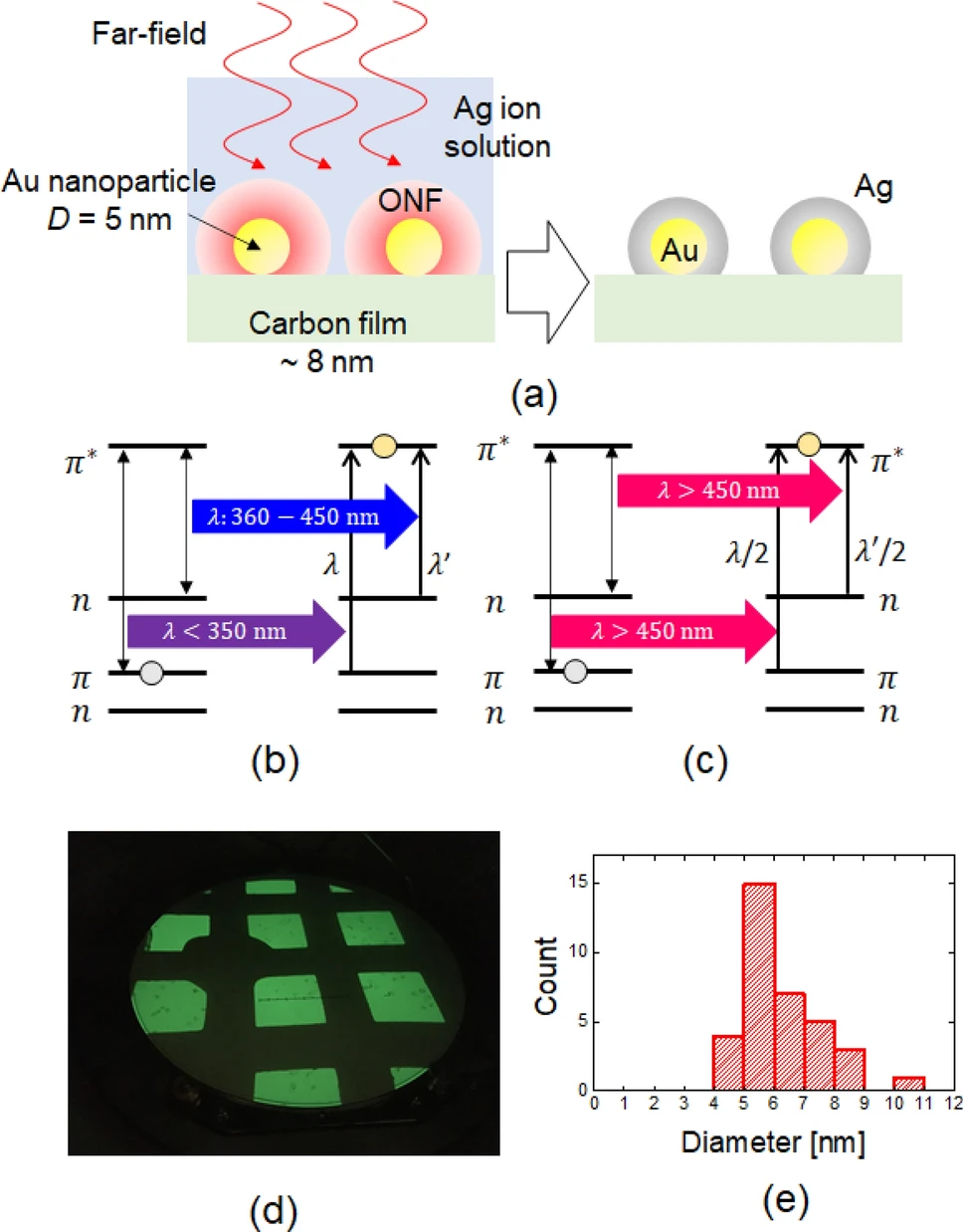
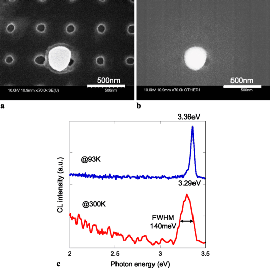
abstract = {By using gold (Au) nanoparticles (NPs) as an optical near-field source under far-field illumination in combination with a silver (Ag) ion solution containing a photoinitiator, we coated Ag on Au NPs using a near-field (NF)-assisted process. We evaluated the change in the size of the NPs using transmission electron microscopy. Evaluation of the synthesized Ag volume over illumination power confirmed the squared power dependence of the NP volume with illumination using 808 nm light, i.e., a wavelength longer than the absorption edge wavelength of the photoinitiator molecules. The rate of volume increase was much lower than the plasmonic field enhancement effect. Therefore, the squared power dependency of the volume increase using a wavelength longer than the absorption edge wavelength originated from NF-assisted second-harmonic generation and the resulting excitation.},
keywords = {First, Nanophotonic fabrication, Near-field effect, SHG},
pubstate = {published},
tppubtype = {article}
}
2019

Takashi Yatsui
Recent improvement of silicon absorption in opto-electric devices Journal Article
In: Opto-Electronic Advances, vol. 2, no. 10, pp. 190023, 2019, (review article, selected as cover story).
Abstract | Links | BibTeX | タグ: Direct wave-vector excitation, First, First principle calculation, Indirect band gap, Near-field effect, Plasmon, Review, Si
@article{OEA_RefItem:1,

title = {Recent improvement of silicon absorption in opto-electric devices},

author = {Takashi Yatsui},

doi = {10.29026/oea.2019.190023},

year  = {2019},

date = {2019-10-01},

urldate = {2019-10-01},

journal = {Opto-Electronic Advances},

volume = {2},

number = {10},

pages = {190023},

publisher = {OEA},

abstract = {Silicon dominates the contemporary electronic industry. However, being an indirect band-gap material, it is a poor absorber of light, which decreases the efficiency of Si-based photodetectors and photovoltaic devices. This review highlights recent studies performed towards improving the optical absorption of Si. A summary of recent theoretical approaches based on the first principle calculation has been provided. It is followed by an overview of recent experimental approaches including scattering, plasmon, hot electron, and near-field effects. The article concludes with a perspective on the future research direction of Si-based photodetectors and photovoltaic devices.},

note = {review article, selected as cover story},

keywords = {Direct wave-vector excitation, First, First principle calculation, Indirect band gap, Near-field effect, Plasmon, Review, Si},

pubstate = {published},

tppubtype = {article}

}
Takashi Yatsui, Syunsuke Okada, Tatsuya Takemori, Takumi Sato, Kota Saichi, Tatsuro Ogamoto, Shohei Chiashi, Shigeo Maruyama, Masashi Noda, Kazuhiro Yabana, Kenji Iida, Katsuyuki Nobusada
Enhanced photo-sensitivity in a Si photodetector using a near-field assisted excitation Journal Article
In: Communications Physics, vol. 2, pp. 62, 2019.
Abstract | Links | BibTeX | タグ: Direct wave-vector excitation, First, Selected, Si photodetector
@article{yatsui2019Si,

title = {Enhanced photo-sensitivity in a Si photodetector using a near-field assisted excitation},

author = {Takashi Yatsui and Syunsuke Okada and Tatsuya Takemori and Takumi Sato and Kota Saichi and Tatsuro Ogamoto and Shohei Chiashi and Shigeo Maruyama and Masashi Noda and Kazuhiro Yabana and Kenji Iida and Katsuyuki Nobusada},

doi = {10.1038/s42005-019-0173-1},

year  = {2019},

date = {2019-06-01},

journal = {Communications Physics},

volume = {2},

pages = {62},

publisher = {Springer Nature},

abstract = {Silicon is an indispensable material in electric device technology. However, Si is an indirect bandgap material; therefore, its excitation efficiency, which requires phonon assistance, is low under propagating far-field light. To improve the excitation efficiency, herein we performed optical near-field excitation, which is confined in a nano-scale, where the interband transitions between different wave numbers are excited according to the uncertainty principle; thus, optical near-field can directly excite the carrier in the indirect bandgap. To evaluate the effect of optical near-field confined in a nano-scale, we fabricate the lateral Si p-n junction with Au nanoparticles as sources to generate the field confinement. We observed a 47.0 % increase in the photo-sensitivity rate. In addition, by using the thin lateral p-n junction, which eliminates the far-field excitation, we confirmed a 42.3 % increase in the photo-sensitivity rate.},

keywords = {Direct wave-vector excitation, First, Selected, Si photodetector},

pubstate = {published},

tppubtype = {article}

}
Takashi Yatsui, Yusuke Nakahira, Yuki Nakamura, Tatsuki Morimoto, Yuma Kato, Muneaki Yamamoto, Tomoko Yoshida, Kenji Iida, Katsuyuki Nobusada
Realization of red shift of absorption spectra using optical near-field effect Journal Article
In: Nanotechnology, vol. 30, no. 34, pp. 34LT02, 2019.
Abstract | Links | BibTeX | タグ: CO2 reduction, First, Near-field effect
@article{Yatsui_2019,

title = {Realization of red shift of absorption spectra using optical near-field effect},

author = {Takashi Yatsui and Yusuke Nakahira and Yuki Nakamura and Tatsuki Morimoto and Yuma Kato and Muneaki Yamamoto and Tomoko Yoshida and Kenji Iida and Katsuyuki Nobusada},

doi = {10.1088/1361-6528/ab2092},

year  = {2019},

date = {2019-06-01},

journal = {Nanotechnology},

volume = {30},

number = {34},

pages = {34LT02},

publisher = {IOP Publishing},

abstract = {In many applications such as CO2 reduction and water splitting, high-energy photons in the ultraviolet region are required to complete the chemical reactions. However, to realize sustainable development, the photon energies utilized must be lower than the absorption edge of the materials including the metal complex for CO2 reduction, the electrodes for water splitting, because of the huge amount of lower energy than the visible region received from the sun. In the previous works, we had demonstrated that optical near-fields (ONFs) could realize chemical reactions, by utilizing photon energies much lower than the absorption edge because of the spatial non-uniformity of the electric field. In this paper, we demonstrate that an ONF can realize the red shift of the absorption spectra of the metal-complex material for photocatalytic reduction. By attaching the metal complex to ZnO nano-crystalline aggregates with nano-scale protrusions, the absorption spectra by using diffuse reflection of the metal complex can be shifted to a longer wavelength by 10.6 nm. The results of computational studies based on a first-principles computational program including the ONF effect provide proof of the increase in the absorption of the metal complex at lower photon energies. Since the near-field assisted field increase improves the carrier excitation in the metal-complex materials, this effect may be universal and it could applicable to CO2 reduction using the other metal-complex materials, as well as to the other photo excitation process including water splitting.},

keywords = {CO2 reduction, First, Near-field effect},

pubstate = {published},

tppubtype = {article}

}
2017
Takashi Yatsui, Hiroshi Saito, Katsuhiro Nishioka, Benjamin Leuschel, Olivier Soppera, Katsuyuki Nobusada
Effects of a power and photon energy of incident light on near-field etching properties Journal Article
In: Applied Physics A, vol. 123, no. 12, pp. 751, 2017.
Abstract | Links | BibTeX | タグ: First, Nanophotonic fabrication, Near-field etching
@article{2017yatsuiAPA,

title = {Effects of a power and photon energy of incident light on near-field etching properties},

author = {Takashi Yatsui and Hiroshi Saito and Katsuhiro Nishioka and Benjamin Leuschel and Olivier Soppera and Katsuyuki Nobusada},

doi = {10.1007/s00339-017-1361-z},

year  = {2017},

date = {2017-12-01},

journal = {Applied Physics A},

volume = {123},

number = {12},

pages = {751},

publisher = {Springer Nature},

abstract = {We developed a near-field etching technique for realizing an ultra-flat surfaces of various materials and structures. To elucidate the near-field etching properties, we have investigated the effects of power and the photon energy of the incident light. First, we established theoretically that an optical near-field with photon energy lower than the absorption edge of the molecules can induce molecular vibrations. We used nanodiamonds to study the power dependence of the near-field etching properties. From the topological changes of the nanodiamonds, we confirmed the linear-dependence of the etching volume with the incident power. Furthermore, we studied the photon energy dependence using TiO2 nanostriped structures, which revealed that a lower photon energy results in a lower etching rate.},

keywords = {First, Nanophotonic fabrication, Near-field etching},

pubstate = {published},

tppubtype = {article}

}
Takashi Yatsui, Hiroshi Saito, Katsuyuki Nobusada
Angstrom-scale flatness using selective nanoscale etching Journal Article
In: Beilstein Journal of Nanotechnology, vol. 123, pp. 751, 2017.
Abstract | Links | BibTeX | タグ: First, Nanophotonic fabrication, Near-field etching, Wet etching
@article{2017yatsuiBJ,

title = {Angstrom-scale flatness using selective nanoscale etching},

author = {Takashi Yatsui and Hiroshi Saito and Katsuyuki Nobusada},

doi = {10.3762/bjnano.8.217},

year  = {2017},

date = {2017-10-01},

journal = {Beilstein Journal of Nanotechnology},

volume = {123},

pages = {751},

publisher = {Beilstein-Institut.},

abstract = {The realization of flat surfaces on the angstrom scale is required in advanced devices to avoid loss due to carrier (electron and/or photon) scattering. In this work, we have developed a new surface flattening method that involves near-field etching, where optical near-fields (ONFs) act to dissociate the molecules. ONFs selectively generated at the apex of protrusions on the surface selectively etch the protrusions. To confirm the selective etching of the nanoscale structure, we compared near-field etching using both gas molecules and ions in liquid phase. Using two-dimensional Fourier analysis, we found that near-field etching is an effective way to etch on the scale of less than 10 nm for both wet and dry etching techniques. In addition, near-field dry etching may be effective for the selective etching of nanoscale structures with large mean free path values.},

keywords = {First, Nanophotonic fabrication, Near-field etching, Wet etching},

pubstate = {published},

tppubtype = {article}

}

Takashi Yatsui, Maiku Yamaguchi, Katsuyuki Nobusada
Nano-scale chemical reactions based on non-uniform optical near-fields and their applications Journal Article
In: Progress in Quantum Electronics, vol. 55, pp. 166 - 194, 2017, ISSN: 0079-6727, (review article).
Abstract | Links | BibTeX | タグ: Artificial photosynthesis, First, Near-field etching, Non-uniform optical near field, Photodissociation path with two-step excitation, Review, Selected, SHG
@article{YATSUI2017166,

title = {Nano-scale chemical reactions based on non-uniform optical near-fields and their applications},

author = {Takashi Yatsui and Maiku Yamaguchi and Katsuyuki Nobusada},

doi = {10.1016/j.pquantelec.2017.06.001},

issn = {0079-6727},

year  = {2017},

date = {2017-09-01},

journal = {Progress in Quantum Electronics},

volume = {55},

pages = {166 - 194},

abstract = {Interaction between light and materials is essential in the physics underlying all optical devices, including light emitting devices such as light emitting diodes and lasers, photo-voltaic devices, and photo-synthesis systems. The demand for higher light utilization efficiency is becoming increasingly important for advanced optical devices. This is because, when feature size is smaller than the incident light wavelength, photons cannot couple with devices efficiently. In this paper, we review recent progress regarding a unique phenomenon at the nano scale and its applications. First, we summarize the development of light–matter interactions at the nano-scale. Second, we review recent theoretical works focusing on optical near fields in which unique phenomena arise from non-uniform optical fields. We then review several recent developments based on the near-field effect, including artificial photosynthesis and near-field etching for realization of angstrom-scale fattened surfaces. Finally, we discuss the future outlook for these technologies.},

note = {review article},

keywords = {Artificial photosynthesis, First, Near-field etching, Non-uniform optical near field, Photodissociation path with two-step excitation, Review, Selected, SHG},

pubstate = {published},

tppubtype = {article}

}
2016
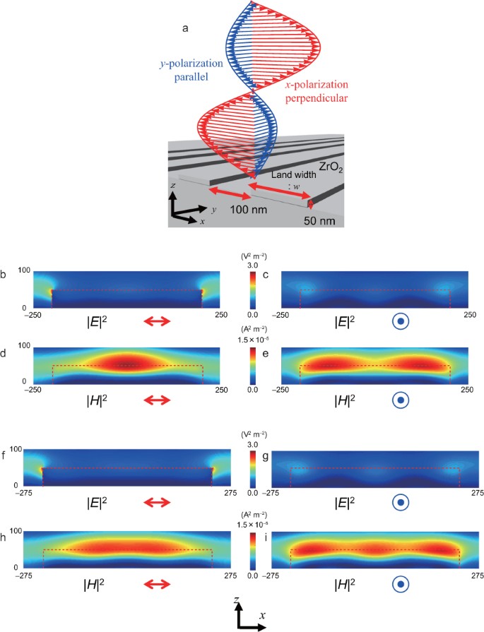
Takashi Yatsui, Toshiki Tsuboi, Maiku Yamaguchi, Katsuyuki Nobusada, Satoshi Tojo, Fabrice Stehlin, Olivier Soppera, Daniel Bloch
Optically controlled magnetic-field etching on the nano-scale Journal Article
In: Light: Science & Applications, vol. 5, pp. e16054, 2016.
Abstract | Links | BibTeX | タグ: First, Nanophotonic fabrication, Near-field etching, Selected
@article{2016YatsuiLST,

title = {Optically controlled magnetic-field etching on the nano-scale},

author = {Takashi Yatsui and Toshiki Tsuboi and Maiku Yamaguchi and Katsuyuki Nobusada and Satoshi Tojo and Fabrice Stehlin and Olivier Soppera and Daniel Bloch},

url = {https://www.altmetric.com/details/6399772},

doi = {10.1038/lsa.2016.54},

year  = {2016},

date = {2016-03-25},

journal = {Light: Science & Applications},

volume = {5},

pages = {e16054},

publisher = {Springer Nature},

abstract = {Electric and magnetic fields play an important role in both chemical and physical reactions. However, since the coupling efficiency between magnetic fields and electrons is low in comparison with that between electric fields and electrons in the visible wavelength region, the magnetic field is negligible in photo-induced reactions. Here, we performed photo-etching of ZrO2 nano-stripe structures, and identified an etching-property polarisation dependence. Specifically, the etching rate and etched profiles depend on the structure width. To evaluate this polarisation-dependent etching, we performed numerical calculations using a finite-difference time-domain method. Remarkably, the numerical results revealed that the polarisation-dependent etching properties were determined by the magnetic field distributions, rather than the electric field distributions. As nano-scale structures induce a localised magnetic field, the discovery of this etching dependence on the magnetic field is expected to introduce a new perspective on advanced nano-scale structure fabrication.},

keywords = {First, Nanophotonic fabrication, Near-field etching, Selected},

pubstate = {published},

tppubtype = {article}

}
Takashi Yatsui, Kazunori Kuribara, Tsuyoshi Sekitani, Takao Someya, Mamoru Yoshimoto
Temperature-modulated annealing of c-plane sapphire for long-range-ordered atomic steps Journal Article
In: Journal of Physics D: Applied Physics, vol. 49, no. 11, pp. 115302, 2016.
Abstract | Links | BibTeX | タグ: chocolate, First, sapphire, tempering
@article{Yatsui_2016,

title = {Temperature-modulated annealing of c-plane sapphire for long-range-ordered atomic steps},

author = {Takashi Yatsui and Kazunori Kuribara and Tsuyoshi Sekitani and Takao Someya and Mamoru Yoshimoto},

doi = {10.1088/0022-3727/49/11/115302},

year  = {2016},

date = {2016-03-23},

urldate = {2016-03-23},

journal = {Journal of Physics D: Applied Physics},

volume = {49},

number = {11},

pages = {115302},

publisher = {IOP Publishing},

abstract = {High-quality single-crystalline sapphire is used to prepare various semiconductors because of its thermal stability. Here, we applied the tempering technique, which is well known in the production of chocolate, to prepare a sapphire substrate. Surprisingly, we successfully realised millimetre-range ordering of the atomic step of the sapphire substrate. We also obtained a sapphire atomic step with nanometre-scale uniformity in the terrace width and atomic-step height. Such sapphire substrates will find applications in the preparation of various semiconductors and devices.},

keywords = {chocolate, First, sapphire, tempering},

pubstate = {published},

tppubtype = {article}

}
2015

Takashi Yatsui, Wataru Nomura, Motoichi Ohtsu
Realization of Ultraflat Plastic Film Using Dressed-Photon-Phonon-Assisted Selective Etching of Nanoscale Structures Journal Article
In: Advances in Optical Technologies, vol. 2015, pp. 701802, 2015.
Abstract | Links | BibTeX | タグ: First, Nanophotonic fabrication, Near-field etching
@article{2015Plastic,

title = {Realization of Ultraflat Plastic Film Using Dressed-Photon-Phonon-Assisted Selective Etching of Nanoscale Structures},

author = {Takashi Yatsui and Wataru Nomura and Motoichi Ohtsu},

doi = {10.1155/2015/701802},

year  = {2015},

date = {2015-02-01},

urldate = {2015-02-01},

journal = {Advances in Optical Technologies},

volume = {2015},

pages = {701802},

abstract = {We compared dressed-photon-phonon (DPP) etching to conventional photochemical etching and, using a numerical analysis of topographic images of the resultant etched polymethyl methacrylate (PMMA) substrate, we determined that the DPP etching resulted in the selective etching of smaller scale structures in comparison with the conventional photochemical etching. We investigated the wavelength dependence of the PMMA substrate etching using an O2 gas. As the dissociation energy of O2 is 5.12 eV, we applied a continuous-wave (CW) He-Cd laser ( 325 nm, 3.81 eV) for the DPP etching and a 5th-harmonic Nd:YAG laser (213  nm, 5.82 eV) for the conventional photochemical etching. From the obtained atomic force microscope images, we confirmed a reduction in surface roughness, Ra, in both cases. However, based on calculations involving the standard deviation of the height difference function, we confirmed that the conventional photochemical etching method etched the larger scale structures only, while the DPP etching process selectively etched the smaller scale features.},

keywords = {First, Nanophotonic fabrication, Near-field etching},

pubstate = {published},

tppubtype = {article}

}
2014
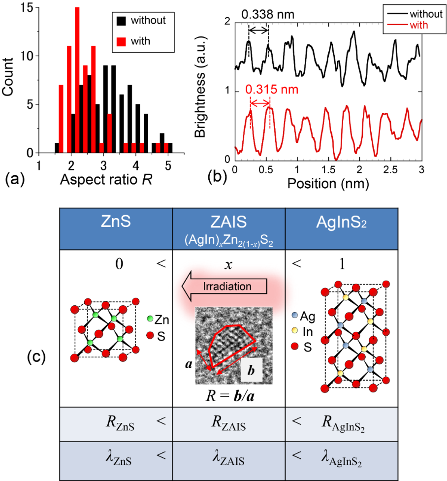
Takashi Yatsui, Fumihiro Morigaki, Tadashi Kawazoe
Controlling the optical and structural properties of ZnS-AgInS2 nanocrystals using photo-induced process Journal Article
In: Beilstein Journal of Nanotechnology, vol. 5, pp. 1767-1773, 2014.
Abstract | Links | BibTeX | タグ: First, Nanophotonic fabrication, ZAIS
@article{2014ZAISBJ,

title = {Controlling the optical and structural properties of ZnS-AgInS2 nanocrystals using photo-induced process},

author = {Takashi Yatsui and Fumihiro Morigaki and Tadashi Kawazoe},

doi = {10.3762/bjnano.5.187},

year  = {2014},

date = {2014-10-01},

journal = {Beilstein Journal of Nanotechnology},

volume = {5},

pages = {1767-1773},

publisher = {Beilstein-Institut.},

abstract = {ZnS-AgInS2 (ZAIS) solid-solution nanocrystals are promising materials for nanophotonic devices in the visible region because of their low toxicity and good emission properties. We developed a technique of photo-induced synthesis to control the size and composition of the ZAIS nanocrystals. This method successfully decreased the defect levels, as well as the size and size variation of ZAIS nanocrystals by controlling the excitation wavelength during synthesis. Detailed analysis of transmission electron microscope images confirmed that the photo-induced synthesis yielded a high crystallinity of the ZAIS nanocrystals with small variations in size and content.},

keywords = {First, Nanophotonic fabrication, ZAIS},

pubstate = {published},

tppubtype = {article}

}

Takashi Yatsui, Daisuke Takeuchi, Satoshi Koizumi, Kazuki Sato, Kohei Tsuzuki, Takayuki Iwasaki, Mutsuko Hatano, Toshiharu Makino, Masahiko Ogura, Hiromitsu Kato, Hideyo Okushi, Satoshi Yamasaki
Polarization-controlled dressed-photon–phonon etching of patterned diamond structures Journal Article
In: physica status solidi (a), vol. 211, no. 10, pp. 2339-2342, 2014.
Abstract | Links | BibTeX | タグ: Diamond, First, Nanophotonic fabrication, Near-field etching
@article{doi:10.1002/pssa.201431161,

title = {Polarization-controlled dressed-photon–phonon etching of patterned diamond structures},

author = {Takashi Yatsui and Daisuke Takeuchi and Satoshi Koizumi and Kazuki Sato and Kohei Tsuzuki and Takayuki Iwasaki and Mutsuko Hatano and Toshiharu Makino and Masahiko Ogura and Hiromitsu Kato and Hideyo Okushi and Satoshi Yamasaki},

doi = {10.1002/pssa.201431161},

year  = {2014},

date = {2014-10-01},

journal = {physica status solidi (a)},

volume = {211},

number = {10},

pages = {2339-2342},

abstract = {To realize an ultra-flat diamond surface with a three-dimensional (3D) structure, we performed dressed-photon–phonon (DPP) etching. A DPP is generated on nano-scale protrusions. Hence, the generation of DPPs results in selective removal of nano-scale protrusions, thereby achieving an ultra-flat surface even on the sidewall of a diamond mesa structure. By controlling the polarization of the incident light, a smooth diamond mesa structure sidewall was obtained, and a higher etching rate was obtained with a perpendicular polarization on the corrugations. In addition, by selective deposition of n-layer diamond on the p-layer diamond mesa structure, smooth n-layer diamond was confirmed on the DPP etched sidewall. Schematic of dressed-photon–phonon (DPP) etching on the sidewall: (a) before and (b) after etching, in which DPP selectively generates on the corrugations and etching automatically stops when the surface was smooth. Scanning electron microscopy image of the selective deposition of the n-layer (c) without and (d) with the DPP etched sidewall.},

keywords = {Diamond, First, Nanophotonic fabrication, Near-field etching},

pubstate = {published},

tppubtype = {article}

}
Takashi Yatsui, Wataru Nomura, Takaaki Mano, Hideki Miyazaki, Kazuaki Sakoda, Tadashi Kawazoe, Motoichi Ohtsu
Emission from a dipole-forbidden energy state in a GaAs quantum-ring induced by dressed photon Journal Article
In: Applied Physics A, vol. 115, no. 1, pp. 1-4, 2014.
Abstract | Links | BibTeX | タグ: First, GaAs, Non-uniform optical near field, Quantum-ring
@article{2014YatsuiGaAsAPA,

title = {Emission from a dipole-forbidden energy state in a GaAs quantum-ring induced by dressed photon},

author = {Takashi Yatsui and Wataru Nomura and Takaaki Mano and Hideki Miyazaki and Kazuaki Sakoda and Tadashi Kawazoe and Motoichi Ohtsu},

doi = {10.1007/s00339-013-7905-y},

year  = {2014},

date = {2014-04-01},

urldate = {2014-04-01},

journal = {Applied Physics A},

volume = {115},

number = {1},

pages = {1-4},

publisher = {Springer Nature},

abstract = {The emission intensity from the dipole-forbidden state in a GaAs quantum-ring was increased via close proximity with an aperture fiber probe to induce a near-field interaction between the probe apex and the quantum-ring. As a result, a significant decrease was observed in the decay time of the emission from a dipole-forbidden energy state.},

keywords = {First, GaAs, Non-uniform optical near field, Quantum-ring},

pubstate = {published},

tppubtype = {article}

}
Takashi Yatsui, Tsubasa Imoto, Takahiro Mochizuki, Kokoro Kitamura, Tadashi Kawazoe
Dressed-photon–phonon (DPP)-assisted visible- and infrared-light water splitting Journal Article
In: Scientific Reports, vol. 4, pp. 4561, 2014.
Abstract | Links | BibTeX | タグ: First, Non-uniform optical near field, Water splitting, ZnO
@article{2014water,

title = {Dressed-photon–phonon (DPP)-assisted visible- and infrared-light water splitting},

author = {Takashi Yatsui and Tsubasa Imoto and Takahiro Mochizuki and Kokoro Kitamura and Tadashi Kawazoe},

doi = {10.1038/srep04561},

year  = {2014},

date = {2014-04-01},

journal = {Scientific Reports},

volume = {4},

pages = {4561},

publisher = {Springer Nature},

abstract = {A dressed-phonon–phonon (DPP) assisted photocatalyst reaction was carried out to increase the visible light responsibility, where the photon energy of the radiation, which ranged from visible to infrared light is less than band gap energy of the photocatalyst (ZnO, 3.3 eV). The dependence of the photocurrent on excitation power indicated that two-step excitation occurred in DPP-assisted process. A cathodoluminescence measurement also supported the conclusion that the visible- and infrared-light excitation originated from DPP excitation, not from defect states in the ZnO nanorod photocatalyst.},

keywords = {First, Non-uniform optical near field, Water splitting, ZnO},

pubstate = {published},

tppubtype = {article}

}
2013

Takashi Yatsui, Wataru Nomura, Fabrice Stehlin, Olivier Soppera, Makoto Naruse, Motoichi Ohtsu
Challenge in realizing ultraflat material surfaces Journal Article
In: Beilstein Journal of Nanotechnology, vol. 4, pp. 875-885, 2013, (review article).
Abstract | Links | BibTeX | タグ: First, Nanophotonic fabrication, Near-field etching, Review, Selected
@article{2013yatsuiBJrev,
title = {Challenge in realizing ultraflat material surfaces},
author = {Takashi Yatsui and Wataru Nomura and Fabrice Stehlin and Olivier Soppera and Makoto Naruse and Motoichi Ohtsu},
doi = {10.3762/bjnano.4.99},
year = {2013},
date = {2013-12-01},
journal = {Beilstein Journal of Nanotechnology},
volume = {4},
pages = {875-885},
publisher = {Beilstein-Institut.},
abstract = {The laser-induced damage threshold (LIDT) is widely used as an index for evaluating an optical componentfs resistance to laser light. However, a degradation in the performance of an optical component is also caused by continuous irradiation with laser light having an energy density below the LIDT. Therefore, here we focused on the degradation in performance of an optical component caused by continuous irradiation with femtosecond laser light having a low energy density, i.e.Ultraflat surface substrates are required to achieve an optimal performance of future optical, electronic, or optoelectronic devices for various applications, because such surfaces reduce the scattering loss of photons, electrons, or both at the surfaces and interfaces. In this paper, we review recent progress toward the realization of ultraflat materials surfaces. First, we review the development of surface-flattening techniques. Second, we briefly review the dressed photon-phonon (DPP), a nanometric quasiparticle that describes the coupled state of a photon, an electron, and a multimode-coherent phonon. Then, we review several recent developments based on DPP-photochemical etching and desorption processes, which have resulted in angstrom-scale flat surfaces. To confirm that the superior flatness of these surfaces that originated from the DPP process, we also review a simplified mathematical model that describes the scale-dependent effects of optical near-fields. Finally, we present the future outlook for these technologies.},
note = {review article},
keywords = {First, Nanophotonic fabrication, Near-field etching, Review, Selected},
pubstate = {published},
tppubtype = {article}
}
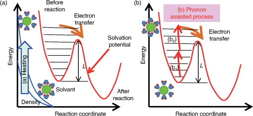
Takashi Yatsui, Kazaunori Iijima, Tsubasa Imoto, Kokoro Kitamura, Tadashi Kawazoe
Phonon-assisted near-field activation of electron transfer Journal Article
In: Journal of Nanophotonics, vol. 7, no. 1, pp. 1 – 8, 2013.
Abstract | Links | BibTeX | タグ: Absorption, Electrodes, First, Nanostructuring, Non-uniform optical near field, Platinum, sapphire
@article{10.1117/1.JNP.7.073796,

title = {Phonon-assisted near-field activation of electron transfer},

author = {Takashi Yatsui and Kazaunori Iijima and Tsubasa Imoto and Kokoro Kitamura and Tadashi Kawazoe},

doi = {10.1117/1.JNP.7.073796},

year  = {2013},

date = {2013-09-01},

journal = {Journal of Nanophotonics},

volume = {7},

number = {1},

pages = {1 -- 8},

publisher = {SPIE},

abstract = {An optical near field should promote phonon-assisted multiple excitation in nanoscale structures. With the phonon-assisted process, greater catalytic activity is expected without heating. To confirm this effect, photo-induced current generation using platinum black electrodes in ferricyanide solution (an absorption band-edge wavelength of 470 nm) under visible light irradiation continuous wave [(CW), λ=532  nm ] was observed. Higher order dependence of the generated current density on the incident light power was observed, indicating two-step activation of electron transfer, which originated from the phonon-assisted near-field effect on the nanostructured surface of the electrode.},

keywords = {Absorption, Electrodes, First, Nanostructuring, Non-uniform optical near field, Platinum, sapphire},

pubstate = {published},

tppubtype = {article}

}
2012
Takashi Yatsui, Wataru Nomura, Makoto Naruse, Motoichi Ohtsu
Realization of an atomically flat surface of diamond using dressed photon–phonon etching Journal Article
In: Journal of Physics D: Applied Physics, vol. 45, no. 47, pp. 475302, 2012.
Abstract | Links | BibTeX | タグ: Diamond, First, Nanophotonic fabrication, Near-field etching
@article{Yatsui_2012,

title = {Realization of an atomically flat surface of diamond using dressed photon–phonon etching},

author = {Takashi Yatsui and Wataru Nomura and Makoto Naruse and Motoichi Ohtsu},

url = {https://doi.org/10.1088%2F0022-3727%2F45%2F47%2F475302},

doi = {10.1088/0022-3727/45/47/475302},

year  = {2012},

date = {2012-11-01},

journal = {Journal of Physics D: Applied Physics},

volume = {45},

number = {47},

pages = {475302},

publisher = {IOP Publishing},

abstract = {We obtained an atomically flat diamond surface following dressed photon–phonon (DPP) etching using 3.81 eV light and O2 gas. We obtained a surface roughness (Ra) of 0.154 nm for Ib-type (1 1 1) diamond and 0.096 nm for Ib-type (1 0 0) diamond. To evaluate the surface roughness, we grouped the surface into bins of width l and introduced the standard deviation of the height difference function for a given separation l, which allowed us to determine the height variation of the surface. Based on the calculation of standard deviation, the conventional adiabatic photochemical reaction did not remove the small surface features, while DPP etching decreased the surface roughness for all length scales.},

keywords = {Diamond, First, Nanophotonic fabrication, Near-field etching},

pubstate = {published},

tppubtype = {article}

}

Takashi Yatsui, Akira Ishikawa, Kiyoshi Kobayashi, Akira Shojiguchi, Suguru Sangu, Tadashi Kawazoe, Motoichi Ohtsu, Jinkyoung Yoo, Gyu-Chul Yi
Superradiance from one-dimensionally aligned ZnO nanorod multiple-quantum-well structures Journal Article
In: Applied Physics Letters, vol. 100, no. 23, pp. 233118, 2012.
Abstract | Links | BibTeX | タグ: First, nanorod, Superradiance, ZnO
@article{doi:10.1063/1.4725514,

title = {Superradiance from one-dimensionally aligned ZnO nanorod multiple-quantum-well structures},

author = {Takashi Yatsui and Akira Ishikawa and Kiyoshi Kobayashi and Akira Shojiguchi and Suguru Sangu and Tadashi Kawazoe and Motoichi Ohtsu and Jinkyoung Yoo and Gyu-Chul Yi},

doi = {10.1063/1.4725514},

year  = {2012},

date = {2012-05-01},

urldate = {2012-05-01},

journal = {Applied Physics Letters},

volume = {100},

number = {23},

pages = {233118},

abstract = {Using one-dimensionally aligned ZnO nanorod multiple-quantum-well structures (MQWs), we observed a superradiance, i.e., a cooperative spontaneous emission. We confirmed that the excitation power dependence of the emissions from the MQWs originated from the coherent coupling of the QWs due to the well organization at nanoscale. We identified two QWs with cooperative emission. Additionally, we evaluated the number of coherently coupled QWs sets of four that resulted in the superradiance. Our findings provide criteria for designing nanoscale synergetic devices without the use of an external cavity.},

keywords = {First, nanorod, Superradiance, ZnO},

pubstate = {published},

tppubtype = {article}

}
Takashi Yatsui, Kosuke Nakanishi, Kokoro Kitamura, Motoichi Ohtsu
Room-temperature growth of high-quality ZnO nanocrystals using a dressed-photon-assisted near-field process Journal Article
In: Applied Physics B, vol. 107, no. 3, pp. 637-641, 2012.
Abstract | Links | BibTeX | タグ: First, Near-field effect, ZnO
@article{2012yatsuiAPB,

title = {Room-temperature growth of high-quality ZnO nanocrystals using a dressed-photon-assisted near-field process},

author = {Takashi Yatsui and Kosuke Nakanishi and Kokoro Kitamura and Motoichi Ohtsu},

doi = {10.1007/s00340-012-5076-8},

year  = {2012},

date = {2012-05-01},

journal = {Applied Physics B},

volume = {107},

number = {3},

pages = {637-641},

publisher = {Springer Nature},

abstract = {Single-crystalline ZnO nanocrystals were fabricated by room-temperature photo-chemical vapor deposition (PCVD). We further enhanced the growth of high-quality single-crystalline ZnO nanocrystals using dressed photons and phonons (DPPs). This resulted in greater position control and the growth of high-quality ZnO nanocrystals. The ZnO nanocrystals produced with DPPs had excellent cathodoluminescence characteristics, indicating that the near-field PCVD process could be a promising technique for nanophotonic integrated circuit production.},

keywords = {First, Near-field effect, ZnO},

pubstate = {published},

tppubtype = {article}

}

Takashi Yatsui, Masahiro Tsuji, Yang Liu, Tadashi Kawazoe, Motoichi Ohtsu
Emission from a dipole-forbidden energy state in a ZnO quantum dot induced by a near-field interaction with a fiber probe Journal Article
In: Applied Physics Letters, vol. 100, no. 22, pp. 223110, 2012.
Abstract | Links | BibTeX | タグ: First, Near-field effect, QD, ZnO
@article{doi:10.1063/1.4723574,

title = {Emission from a dipole-forbidden energy state in a ZnO quantum dot induced by a near-field interaction with a fiber probe},

author = {Takashi Yatsui and Masahiro Tsuji and Yang Liu and Tadashi Kawazoe and Motoichi Ohtsu},

doi = {10.1063/1.4723574},

year  = {2012},

date = {2012-05-01},

urldate = {2012-05-01},

journal = {Applied Physics Letters},

volume = {100},

number = {22},

pages = {223110},

abstract = {The emission intensity from the dipole-forbidden state in a spherical quantum dot (QD) was enhanced by introducing an aperture fiber probe close to the ZnO QD to induce a near-field interaction between the probe tip and the QD. The cross-sectional profiles of the photoluminescence intensities of the ground exciton state and the excited exciton states varied spatially in an anti-correlated manner.},

keywords = {First, Near-field effect, QD, ZnO},

pubstate = {published},

tppubtype = {article}

}
2011
Takashi Yatsui, Kazuya Hirata, Yoshinori Tabata, Yumiko Miyake, Yasuyuki Akita, Mamoru Yoshimoto, Wataru Nomura, Tadashi Kawazoe, Makoto Naruse, Motoichi Ohtsu
Self-organized near-field etching of the sidewalls of glass corrugations Journal Article
In: Applied Physics B, vol. 103, no. 3, pp. 527-530, 2011.
Abstract | Links | BibTeX | タグ: First, Nanophotonic fabrication, Near-field etching
@article{2011yatsuiAPBNFE,

title = {Self-organized near-field etching of the sidewalls of glass corrugations},

author = {Takashi Yatsui and Kazuya Hirata and Yoshinori Tabata and Yumiko Miyake and Yasuyuki Akita and Mamoru Yoshimoto and Wataru Nomura and Tadashi Kawazoe and Makoto Naruse and Motoichi Ohtsu},

doi = {10.1007/s00340-011-4569-1},

year  = {2011},

date = {2011-06-01},

journal = {Applied Physics B},

volume = {103},

number = {3},

pages = {527-530},

publisher = {Springer Nature},

abstract = {Using soda-lime glass with a nano-stripe pattern as a test specimen, we demonstrated self-organized near-field etching with a continuum-wave laser (wavelength of 532 nm) light source. Atomic force microscopy confirmed that near-field etching decreases the flank roughness of the corrugations as well as the roughness of the flat surface.},

keywords = {First, Nanophotonic fabrication, Near-field etching},

pubstate = {published},

tppubtype = {article}

}
2010
Takashi Yatsui, Kazuya Hirata, Yoshinori Tabata, Wataru Nomura, Tadashi Kawazoe, Makoto Naruse, Motoichi Ohtsu
In situ real-time monitoring of changes in the surface roughness during nonadiabatic optical near-field etching Journal Article
In: Nanotechnology, vol. 21, no. 35, pp. 355303, 2010.
Abstract | Links | BibTeX | タグ: First, Nanophotonic fabrication, Near-field etching
@article{Yatsuii_2010,

title = {In situ real-time monitoring of changes in the surface roughness during nonadiabatic optical near-field etching},

author = {Takashi Yatsui and Kazuya Hirata and Yoshinori Tabata and Wataru Nomura and Tadashi Kawazoe and Makoto Naruse and Motoichi Ohtsu},

doi = {10.1088/0957-4484/21/35/355303},

year  = {2010},

date = {2010-08-01},

journal = {Nanotechnology},

volume = {21},

number = {35},

pages = {355303},

publisher = {IOP Publishing},

abstract = {We performed in situ real-time monitoring of the change in surface roughness during

self-organized optical near-field etching. During near-field etching of a silica substrate, we detected the scattered light intensity from a continuum wave (CW) laser (λ = 633 nm) in addition to the etching CW laser (λ = 532 nm) light source. We discovered that near-field etching not only decreases surface

roughness, but also increases the number of scatterers, as was confirmed by analyzing the

AFM image. These approaches provide optimization criteria for the etching parameter and

hence for further decreases in surface roughness.},

keywords = {First, Nanophotonic fabrication, Near-field etching},

pubstate = {published},

tppubtype = {article}

}
self-organized optical near-field etching. During near-field etching of a silica substrate, we detected the scattered light intensity from a continuum wave (CW) laser (λ = 633 nm) in addition to the etching CW laser (λ = 532 nm) light source. We discovered that near-field etching not only decreases surface
roughness, but also increases the number of scatterers, as was confirmed by analyzing the
AFM image. These approaches provide optimization criteria for the etching parameter and
hence for further decreases in surface roughness.

Takashi Yatsui, Yang Ryu, Tetsu Morishima, Wataru Nomura, Tadashi Kawazoe, Tetsu Yonezawa, Masao Washizu, Hiroyuki Fujita, Motoichi Ohtsu
Self-assembly method of linearly aligning ZnO quantum dots for a nanophotonic signal transmission device Journal Article
In: Applied Physics Letters, vol. 96, no. 13, pp. 133106, 2010.
Abstract | Links | BibTeX | タグ: First, Nanophotonic device, QD, Self-assembly, ZnO
@article{doi:10.1063/1.3372639,

title = {Self-assembly method of linearly aligning ZnO quantum dots for a nanophotonic signal transmission device},

author = {Takashi Yatsui and Yang Ryu and Tetsu Morishima and Wataru Nomura and Tadashi Kawazoe and Tetsu Yonezawa and Masao Washizu and Hiroyuki Fujita and Motoichi Ohtsu},

url = {https://doi.org/10.1063/1.3372639},

doi = {10.1063/1.3372639},

year  = {2010},

date = {2010-01-01},

urldate = {2010-01-01},

journal = {Applied Physics Letters},

volume = {96},

number = {13},

pages = {133106},

abstract = {We report a self-assembly method that aligns nanometer-sized quantum dots (QDs) into a straight line along which photonic signals can be transmitted by optically near-field effects. ZnO QDs were bound electrostatically to DNA to form a one-dimensional QD chain. The photoluminescence intensity under parallel polarization excitation along the QDs chain was much greater than under perpendicular polarization excitation, indicating an efficient signal transmission along the QD chain. As optical near-field energy can transmit through the resonant energy level, nanophotonic signal transmission devices have a number of potential applications, such as wavelength division multiplexing using QDs of different sizes.},

keywords = {First, Nanophotonic device, QD, Self-assembly, ZnO},

pubstate = {published},

tppubtype = {article}

}
2009
Takashi Yatsui, Shunsuke Yamazaki, Keiichi Ito, Hiroshi Kawamura, Michinobu Mizumura, Tadashi Kawazoe, Motoichi Ohtsu
Increased spatial homogeneity in a light-emitting InGaN thin film using optical near-field desorption Journal Article
In: Applied Physics B, vol. 97, no. 2, pp. 375-378, 2009.
Abstract | Links | BibTeX | タグ: First, GaN, Nanophotonic fabrication, Near-field effect, Self-assembly
@article{2009yatsuiGaNAPB,

title = {Increased spatial homogeneity in a light-emitting InGaN thin film using optical near-field desorption},

author = {Takashi Yatsui and Shunsuke Yamazaki and Keiichi Ito and Hiroshi Kawamura and Michinobu Mizumura and Tadashi Kawazoe and Motoichi Ohtsu},

doi = {10.1007/s00340-009-3757-8},

year  = {2009},

date = {2009-10-01},

journal = {Applied Physics B},

volume = {97},

number = {2},

pages = {375-378},

publisher = {Springer Nature},

abstract = {We report a self-assembly method that produces greater spatial uniformity in InGaN thin films using optical near-field desorption. Spatial homogeneity in the In fraction was reduced by introducing additional light during the photo-enhanced chemical vapor deposition of InGaN. Near-field desorption of InGaN nanoparticles, upon addition depended on the In content of the film, and the photon energy of the illumination source determined the energy of the emitted photons. Since this deposition method is based on a photo-desorption reaction, it can easily be applied to other deposition techniques and used with other semiconductor systems.},

keywords = {First, GaN, Nanophotonic fabrication, Near-field effect, Self-assembly},

pubstate = {published},

tppubtype = {article}

}

Takashi Yatsui, Motoichi Ohtsu
Production of size-controlled Si nanocrystals using self-organized optical near-field chemical etching Journal Article
In: Applied Physics Letters, vol. 95, no. 4, pp. 043104, 2009.
Abstract | Links | BibTeX | タグ: First, Nanophotonic fabrication, Near-field effect, Self-assembly, Si
@article{doi:10.1063/1.3193536,

title = {Production of size-controlled Si nanocrystals using self-organized optical near-field chemical etching},

author = {Takashi Yatsui and Motoichi Ohtsu},

doi = {10.1063/1.3193536},

year  = {2009},

date = {2009-07-24},

urldate = {2009-07-24},

journal = {Applied Physics Letters},

volume = {95},

number = {4},

pages = {043104},

abstract = {We demonstrate the selective photochemical etching of Si in a self-organized manner, which strongly depends on the distribution of the optical near field. This dependence was described by the virtual exciton-phonon-polariton model. The photoluminescence (PL) spectra from the etched Si exhibited a blueshifted PL peak at 1.8 eV, corresponding to Si nanocrystals of 2.8 nm diameter.},

keywords = {First, Nanophotonic fabrication, Near-field effect, Self-assembly, Si},

pubstate = {published},

tppubtype = {article}

}

Takashi Yatsui, Suguru Sangu, Kiyoshi Kobayashi, Tadashi Kawazoe, Motoichi Ohtsu, Jinkyoung Yoo, Gyu-Chul Yi
Nanophotonic energy up conversion using ZnO nanorod double-quantum-well structures Journal Article
In: Applied Physics Letters, vol. 94, no. 8, pp. 083113, 2009.
Abstract | Links | BibTeX | タグ: First, nanorod, Non-uniform optical near field, ZnO
@article{doi:10.1063/1.3090491,

title = {Nanophotonic energy up conversion using ZnO nanorod double-quantum-well structures},

author = {Takashi Yatsui and Suguru Sangu and Kiyoshi Kobayashi and Tadashi Kawazoe and Motoichi Ohtsu and Jinkyoung Yoo and Gyu-Chul Yi},

url = {https://doi.org/10.1063/1.3090491},

doi = {10.1063/1.3090491},

year  = {2009},

date = {2009-02-01},

urldate = {2009-02-01},

journal = {Applied Physics Letters},

volume = {94},

number = {8},

pages = {083113},

abstract = {We report on near-field spectroscopy of ZnO/ZnMgO nanorod double-quantum-well structures (DQWs) for a nanometer-scale photonic device. We observed energy up conversion assisted by the absorption of phonons generated in the ZnO nanorod DQWs. Theoretical calculation of the coherent excitonic excitation of the population with incoherent phonon coupling agrees well with the obtained experimental power dependence of the up conversion efficiency. It should result in an increase in the efficiency of devices, such as photodetectors, solar cells, and so on.},

keywords = {First, nanorod, Non-uniform optical near field, ZnO},

pubstate = {published},

tppubtype = {article}

}
2008
Takashi Yatsui, Kazuya Hirata, Wataru Nomura, Yoshinori Tabata, Motoichi Ohtsu
Realization of an ultra-flat silica surface with angstrom-scale average roughness using nonadiabatic optical near-field etching Journal Article
In: Applied Physics B, vol. 93, no. 1, pp. 55-57, 2008.
Abstract | Links | BibTeX | タグ: First, Nanophotonic fabrication, Near-field etching, Selected
@article{2008yatsuiAPBNFE,

title = {Realization of an ultra-flat silica surface with angstrom-scale average roughness using nonadiabatic optical near-field etching},

author = {Takashi Yatsui and Kazuya Hirata and Wataru Nomura and Yoshinori Tabata and Motoichi Ohtsu},

doi = {10.1007/s00340-008-3142-z},

year  = {2008},

date = {2008-10-01},

journal = {Applied Physics B},

volume = {93},

number = {1},

pages = {55-57},

publisher = {Springer Nature},

abstract = {We propose a new method of optical near-field etching where a nonadiabatic process is applied to a synthetic silica substrate using a continuum wave laser (λ=532 nm) with a Cl2 gas source. Because the absorption band edge energy of Cl2 is higher than the photon energy of the light source, we preclude the conventional adiabatic photochemical reaction. An optical near field, generated on the nanometrically rough substrate, induces the nonadiabatic chemical reaction to the Cl2 molecules and thereby selectively etches away the roughness, leaving an ultra-flat synthetic silica surface with a minimum average surface roughness R a of 1.37 A.},

keywords = {First, Nanophotonic fabrication, Near-field etching, Selected},

pubstate = {published},

tppubtype = {article}

}
Takashi Yatsui, Hyung Su Jeong, Motoichi Ohtsu
Controlling the energy transfer between near-field optically coupled ZnO quantum dots Journal Article
In: Applied Physics B, vol. 93, no. 1, pp. 199-202, 2008.
Abstract | Links | BibTeX | タグ: Electrodes, First, QD, ZnO
@article{2008yatsuiAPBZnO,

title = {Controlling the energy transfer between near-field optically coupled ZnO quantum dots},

author = {Takashi Yatsui and Hyung Su Jeong and Motoichi Ohtsu},

doi = {10.1007/s00340-008-3154-8},

year  = {2008},

date = {2008-10-01},

journal = {Applied Physics B},

volume = {93},

number = {1},

pages = {199-202},

publisher = {Springer Nature},

abstract = {We performed time-resolved spectroscopy of ZnO quantum dots (QD), and observed exciton energy transfer and dissipation between QD via an optical near-field interaction. Two different sizes of ZnO QD with resonant energy levels were mixed to test the energy transfer and dissipation using time-resolved photoluminescence spectroscopy. The estimated energy transfer time was 144 ps. Furthermore, we demonstrated that the ratio of energy transfer between the resonant energy states could be controlled.},

keywords = {Electrodes, First, QD, ZnO},

pubstate = {published},

tppubtype = {article}

}
2007
Takashi Yatsui, Tadashi Kawazoe, Kiyoshi Kobayashi, Motoichi Ohtsu
Near-field components and evaluation of photoluminescence in silicon nanostructures Journal Article
In: Journal of Nanophotonics, vol. 1, no. 1, pp. 011570, 2007.
Abstract | Links | BibTeX | タグ: First, Non-uniform optical near field, Si, silicon
@article{10.1117/1.2794355,

title = {Near-field components and evaluation of photoluminescence in silicon nanostructures},

author = {Takashi Yatsui and Tadashi Kawazoe and Kiyoshi Kobayashi and Motoichi Ohtsu},

doi = {10.1117/1.2794355},

year  = {2007},

date = {2007-09-01},

journal = {Journal of Nanophotonics},

volume = {1},

number = {1},

pages = {011570},

publisher = {SPIE},

abstract = {Using illumination-collection mode optical near-field spectroscopy, a a spectral shift of photoluminescence of silicon (Si) nanocrystals compared with the far-field measurement was observed, due to the near-field coupling of the Si nanocrystals and the probe.},

keywords = {First, Non-uniform optical near field, Si, silicon},

pubstate = {published},

tppubtype = {article}

}
Takashi Yatsui, Wataru Nomura, Motoichi Ohtsu
Metallized slit-shaped pyramidal Si probe with extremely high resolution for 1.5-Tbit/in2 density near-field optical storage Journal Article
In: Journal of Nanophotonics, vol. 1, no. 1, pp. 011550, 2007.
Abstract | Links | BibTeX | タグ: First, near-field optical recording, Optical storage, Si
@article{10.1117/1.2794357,

title = {Metallized slit-shaped pyramidal Si probe with extremely high resolution for 1.5-Tbit/in2 density near-field optical storage},

author = {Takashi Yatsui and Wataru Nomura and Motoichi Ohtsu},

url = {https://doi.org/10.1117/1.2794357},

doi = {10.1117/1.2794357},

year  = {2007},

date = {2007-09-01},

journal = {Journal of Nanophotonics},

volume = {1},

number = {1},

pages = {011550},

publisher = {SPIE},

abstract = {We have developed a near-field optical probe by introducing the metallized pyramidal structure of a Si probe with a slit-shaped tip for high-density optical storage. Numerical analysis using the finite-difference time-domain method showed that the optical spot generated at the aperture measured 13×30 nm. We fabricated a slit-type Si probe and evaluated the spot size using fluorescence imaging of a single dye molecule. The full-width at half maximum of the signal profiles was 16 nm×26 nm, which corresponds to a data density of 1.5 Tbit/in2. Furthermore, a large extinction coefficient depending on the polarization was confirmed.},

keywords = {First, near-field optical recording, Optical storage, Si},

pubstate = {published},

tppubtype = {article}

}
Takashi Yatsui, Jungshik Lim, Tooru Nakamata, Kokoro Kitamura, Motoichi Ohtsu, Gyu-Chul Yi
Low-temperature (~270 oC) growth of vertically aligned ZnO nanorods using photoinduced metal organic vapour phase epitaxy Journal Article
In: Nanotechnology, vol. 18, no. 6, pp. 065606, 2007.
Abstract | Links | BibTeX | タグ: First, nanorod, Near-field effect, ZnO
@article{Yatsui_2007,

title = {Low-temperature (~270 oC) growth of vertically aligned ZnO nanorods using photoinduced metal organic vapour phase epitaxy},

author = {Takashi Yatsui and Jungshik Lim and Tooru Nakamata and Kokoro Kitamura and Motoichi Ohtsu and Gyu-Chul Yi},

doi = {10.1088/0957-4484/18/6/065606},

year  = {2007},

date = {2007-02-01},

journal = {Nanotechnology},

volume = {18},

number = {6},

pages = {065606},

publisher = {IOP Publishing},

abstract = {We successfully produced a drastic decrease in the required growth temperature

of single-crystalline ZnO nanorods, and enabled successful growth of vertically

aligned ZnO nanorods on a Si(100) substrate using photoinduced metal organic

vapour phase epitaxy (MOVPE). We introduced 325 nm light during the MOVPE

growth, and achieved vertical growth of single-crystalline ZnO nanorods

with a hexagonal crystal structure on Si(100) at a growth temperature of

270 °C. The successful low-temperature growth of ZnO nanorods on the Si(100) substrate

described here is a promising step toward designing nanoscale photonic and electronic

devices required by future systems.},

keywords = {First, nanorod, Near-field effect, ZnO},

pubstate = {published},

tppubtype = {article}

}
of single-crystalline ZnO nanorods, and enabled successful growth of vertically
aligned ZnO nanorods on a Si(100) substrate using photoinduced metal organic
vapour phase epitaxy (MOVPE). We introduced 325 nm light during the MOVPE
growth, and achieved vertical growth of single-crystalline ZnO nanorods
with a hexagonal crystal structure on Si(100) at a growth temperature of
270 °C. The successful low-temperature growth of ZnO nanorods on the Si(100) substrate
described here is a promising step toward designing nanoscale photonic and electronic
devices required by future systems.

Takashi Yatsui, Suguru Sangu, Tadashi Kawazoe, Motoichi Ohtsu, Sung Jin An, Jinkyoung Yoo, Gyu-Chul Yi
Nanophotonic switch using ZnO nanorod double-quantum-well structures Journal Article
In: Applied Physics Letters, vol. 90, no. 22, pp. 223110, 2007.
Abstract | Links | BibTeX | タグ: First, Nanophotonic device, Selected, ZnO
@article{doi:10.1063/1.2743949,

title = {Nanophotonic switch using ZnO nanorod double-quantum-well structures},

author = {Takashi Yatsui and Suguru Sangu and Tadashi Kawazoe and Motoichi Ohtsu and Sung Jin An and Jinkyoung Yoo and Gyu-Chul Yi},

doi = {10.1063/1.2743949},

year  = {2007},

date = {2007-01-01},

urldate = {2007-01-01},

journal = {Applied Physics Letters},

volume = {90},

number = {22},

pages = {223110},

abstract = {The authors report on time-resolved near-field spectroscopy of ZnO∕ZnMgO nanorod double-quantum-well structures (DQWs) for a nanometer-scale photonic device. They observed nutation of the population between the resonantly coupled exciton states of DQWs. Furthermore, they demonstrated switching dynamics by controlling the exciton excitation in the dipole-inactive state via an optical near field. The results of time-resolved near-field spectroscopy of isolated DQWs described here are a promising step toward designing a nanometer-scale photonic switch and related devices.},

keywords = {First, Nanophotonic device, Selected, ZnO},

pubstate = {published},

tppubtype = {article}

}
2006
Takashi Yatsui, Motoichi Ohtsu, Sung Jin An, Jinkyoung Yoo, Gyu-Chul Yi
In: Optical Review, vol. 13, no. 4, pp. 218-221, 2006.
Abstract | Links | BibTeX | タグ: First, nanorod, Near-field spectroscopy, ZnO
@article{2006yatsuiOptRev,

title = {Evaluating the quantum confinement effect of isolated ZnO nanorod single-quantum-well structures using near-field ultraviolet photoluminescence spectroscopy},

author = {Takashi Yatsui and Motoichi Ohtsu and Sung Jin An and Jinkyoung Yoo and Gyu-Chul Yi},

doi = {10.1007/s10043-006-0218-z},

year  = {2006},

date = {2006-07-01},

journal = {Optical Review},

volume = {13},

number = {4},

pages = {218-221},

publisher = {Springer Nature},

abstract = {Using low-temperature near-field spectroscopy, we obtained spatially and spectrally resolved photoluminescence (PL) images of individual ZnO nanorod single-quantum-well structures (SQWs) with a spatial resolution of 20 nm. We observed the dependence of the quantum confinement effect of the PL peak on the well width (L aw), from which the linewidths of near-field PL spectra of ZnO nanorod SQWs (L aw = 2.5 and 3.75 nm) were determined to be as narrow as 3 meV. However, near-field PL spectra of individual SQWs with L aw = 5.0 nm exhibited two PL peaks, presumably due to strains or defects in the ZnMgO in the nanorod SQWs. Since the exciton in a quantum structure is an ideal two-level system with long coherence times, our results provide criteria for designing nanophotonic devices.},

keywords = {First, nanorod, Near-field spectroscopy, ZnO},

pubstate = {published},

tppubtype = {article}

}
Takashi Yatsui, Yuuki Nakajima, Wataru Nomura, Motoichi Ohtsu
High-resolution capability of optical near-field imprint lithography Journal Article
In: Applied Physics B, vol. 84, no. 1-2, pp. 265-267, 2006.
Abstract | Links | BibTeX | タグ: First, Imprint, Nanophotonic fabrication, Near-field effect
@article{2006yatsuiAPBimprint,

title = {High-resolution capability of optical near-field imprint lithography},

author = {Takashi Yatsui and Yuuki Nakajima and Wataru Nomura and Motoichi Ohtsu},

doi = {10.1007/s00340-006-2328-5},

year  = {2006},

date = {2006-07-01},

journal = {Applied Physics B},

volume = {84},

number = {1-2},

pages = {265-267},

publisher = {Springer Nature},

abstract = {We propose a novel method to increase the resolution of imprint lithography by introducing strong localization of the optical near-field intensity, depending on the mold structure. By optimizing the thickness of the metallic film on a SiO2 line-and-space (LS) mold without a sidewall coating, we confirmed that the optical near-field strongly localizes at the edge of the mold, using a finite-difference time-domain calculation method. Based on the calculated results, we performed optical near-field imprint lithography using a mold with metallized (20-nm-thick Al without a sidewall coating) SiO2 LS with a 300-nm half-pitch that was 200-nm deep with illumination using the g-line (wavelength of 436 nm), and obtained features as narrow as 50 nm wide.},

keywords = {First, Imprint, Nanophotonic fabrication, Near-field effect},

pubstate = {published},

tppubtype = {article}

}
2005

Takashi Yatsui, Wataru Nomura, Motoichi Ohtsu
Self-Assembly of Size- and Position-Controlled Ultralong Nanodot Chains using Near-Field Optical Desorption Journal Article
In: Nano Letters, vol. 5, no. 12, pp. 2548-2551, 2005, (PMID: 16351213).
Abstract | Links | BibTeX | タグ: First, Nanophotonic fabrication, Plasmon, Selected, Self-assembly
@article{doi:10.1021/nl051898z,

title = {Self-Assembly of Size- and Position-Controlled Ultralong Nanodot Chains using Near-Field Optical Desorption},

author = {Takashi Yatsui and Wataru Nomura and Motoichi Ohtsu},

doi = {10.1021/nl051898z},

year  = {2005},

date = {2005-12-01},

journal = {Nano Letters},

volume = {5},

number = {12},

pages = {2548-2551},

abstract = {We report the self-assembly of a size- and position-controlled ultralong nanodot chain using a novel effect of near-field optical desorption. A sub-100-nm dot chain with a deviation of 5 nm forms at a size based on plasmon resonance, depending on the photon energy; the resulting structure forms a high-transmission-efficiency nanoscale waveguide. Using this method with simple lithographically patterned substrates allows one to increase the throughput of the production of nanoscale structures dramatically at all scales.},

note = {PMID: 16351213},

keywords = {First, Nanophotonic fabrication, Plasmon, Selected, Self-assembly},

pubstate = {published},

tppubtype = {article}

}
Takashi Yatsui, Wataru Nomura, Motoichi Ohtsu
Size-, Position-, and Separation-Controlled One-Dimensional Alignment of Nanoparticles Using an Optical Near Field Journal Article
In: IEICE TRANSACTIONS on Electronics, vol. E88-C, no. 9, pp. 1798-1802, 2005.
Abstract | Links | BibTeX | タグ: First, Nanophotonic fabrication, Self-assembly
@article{2005IEICE,

title = {Size-, Position-, and Separation-Controlled One-Dimensional Alignment of Nanoparticles Using an Optical Near Field},

author = {Takashi Yatsui and Wataru Nomura and Motoichi Ohtsu},

doi = {10.1093/ietele/e88-c.9.1798},

year  = {2005},

date = {2005-09-01},

journal = {IEICE TRANSACTIONS on Electronics},

volume = {E88-C},

number = {9},

pages = {1798-1802},

publisher = {IEICE},

abstract = {Particles several tens of nanometers in size were aligned in the desired positions in a controlled manner by using capillary force interaction and suspension flow. Latex beads 40-nm in diameter were aligned linearly around a 10-um-hole template fabricated by lithography. Further control of their position and separation was realized using colloidal gold nanoparticles by controlling the particle-substrate and particle-particle interactions using an optical near field generated on the edge of a Si wedge, in which the separation of the colloidal gold nanoparticles was controlled by the direction of polarization.},

keywords = {First, Nanophotonic fabrication, Self-assembly},

pubstate = {published},

tppubtype = {article}

}

Takashi Yatsui, Motoichi Ohtsu, Jinkyoung Yoo, Sung Jin An, Gyu-Chul Yi
Near-field measurement of spectral anisotropy and optical absorption of isolated ZnO nanorod single-quantum-well structures Journal Article
In: Applied Physics Letters, vol. 87, no. 3, pp. 033101, 2005.
Abstract | Links | BibTeX | タグ: First, Near-field spectroscopy, QW, ZnO
@article{doi:10.1063/1.1990247,

title = {Near-field measurement of spectral anisotropy and optical absorption of isolated ZnO nanorod single-quantum-well structures},

author = {Takashi Yatsui and Motoichi Ohtsu and Jinkyoung Yoo and Sung Jin An and Gyu-Chul Yi},

doi = {10.1063/1.1990247},

year  = {2005},

date = {2005-07-01},

urldate = {2005-07-01},

journal = {Applied Physics Letters},

volume = {87},

number = {3},

pages = {033101},

abstract = {We report low-temperature near-field spectroscopy of isolated ZnO∕ZnMgO single-quantum-well structures (SQWs) on the end of ZnO nanorod to define their potential for nanophotonics. First, absorption spectra of isolated ZnO∕ZnMgO nanorod SQWs with the Stokes shift as small as 3meV and very sharp photoluminescent peaks indicate that the nanorod SQWs are of very high optical quality. Furthermore, we performed polarization spectroscopy of isolated ZnO SQWs, and observed valence-band anisotropy of ZnO SQWs in photoluminescence spectra directly. Since the exciton in a quantum structure is an ideal two-level system with long coherence times, our results provide criteria for designing nanophotonic devices.},

keywords = {First, Near-field spectroscopy, QW, ZnO},

pubstate = {published},

tppubtype = {article}

}
2004

Takashi Yatsui, Jungshik Lim, Motoichi Ohtsu, Sung Jin An, Gyu-Chul Yi
In: Applied Physics Letters, vol. 85, no. 5, pp. 727-729, 2004.
Abstract | Links | BibTeX | タグ: First, nanorod, Near-field spectroscopy, QW, ZnO
@article{doi:10.1063/1.1776338,

title = {Evaluation of the discrete energy levels of individual ZnO nanorodsingle-quantum-well structures using near-field ultraviolet photoluminescence spectroscopy},

author = {Takashi Yatsui and Jungshik Lim and Motoichi Ohtsu and Sung Jin An and Gyu-Chul Yi},

doi = {10.1063/1.1776338},

year  = {2004},

date = {2004-08-01},

urldate = {2004-08-01},

journal = {Applied Physics Letters},

volume = {85},

number = {5},

pages = {727-729},

abstract = {Spatially and spectrally resolved photoluminescence imaging of individual ZnO∕ZnMgO nanorod single-quantum-well structures (SQWs) with a spatial resolution of 55nm was performed using the optical near-field technique with a metallized UV fiber probe. Using excitation power density-dependent photoluminescence spectra of a ZnO∕ZnMgO SQW nanorod, we observed the discrete energy levels in a ZnO quantum-well layer.},

keywords = {First, nanorod, Near-field spectroscopy, QW, ZnO},

pubstate = {published},

tppubtype = {article}

}
2003
Takashi Yatsui, Akira Takubo, Jungshik Lim, Wataru Nomura, Motonobu Kourogi, Motoichi Ohtsu
Regulating the size and position of deposited Zn nanoparticles by optical near-field desorption using size-dependent resonance Journal Article
In: Applied Physics Letters, vol. 83, no. 9, pp. 1716-1718, 2003.
Abstract | Links | BibTeX | タグ: First, Self-assembly, Size-dependent resonance
@article{doi:10.1063/1.1606883,

title = {Regulating the size and position of deposited Zn nanoparticles by optical near-field desorption using size-dependent resonance},

author = {Takashi Yatsui and Akira Takubo and Jungshik Lim and Wataru Nomura and Motonobu Kourogi and Motoichi Ohtsu},

doi = {10.1063/1.1606883},

year  = {2003},

date = {2003-09-01},

journal = {Applied Physics Letters},

volume = {83},

number = {9},

pages = {1716-1718},

abstract = {We report that optical near-field desorption can dramatically regulate the growth of Zn nanoparticles during optical chemical vapor deposition. The trade off between the deposition due to 3.81 eV optical near-field light and desorption due to 2.54 eV optical near-field light allowed the fabrication of a single 15 nm Zn dot, while regulating its size and position.},

keywords = {First, Self-assembly, Size-dependent resonance},

pubstate = {published},

tppubtype = {article}

}
2002
Takashi Yatsui, Tadashi Kawazoe, Minoru Ueda, Yoh Yamamoto, Motonobu Kourogi, Motoichi Ohtsu
In: Applied Physics Letters, vol. 81, no. 19, pp. 3651-3653, 2002.
Abstract | Links | BibTeX | タグ: First, Near-field effect
@article{doi:10.1063/1.1520337,

title = {Fabrication of nanometric single zinc and zinc oxide dots by the selective photodissociation of adsorption-phase diethylzinc using a nonresonant optical near field},

author = {Takashi Yatsui and Tadashi Kawazoe and Minoru Ueda and Yoh Yamamoto and Motonobu Kourogi and Motoichi Ohtsu},

doi = {10.1063/1.1520337},

year  = {2002},

date = {2002-11-01},

journal = {Applied Physics Letters},

volume = {81},

number = {19},

pages = {3651-3653},

abstract = {We demonstrated a deposition of nanometer-scale Zn dots using the selective photodissociation of adsorption-phase diethylzinc with a nonresonant optical near field, where the photon energy is lower than that of the absorption edge of gas-phase diethylzinc. We achieved nanometric prenucleation by dissociating diethylzinc molecules adsorbed on a substrate. Subsequent deposition was performed by dissociating the adsorbed molecules on the prenucleated Zn. The topographic image of the deposited Zn dot had a full width at half maximum (FWHM) of 25 nm. Furthermore, the photoluminescence intensity distribution from a single ZnO dot fabricated using laser annealing had a FWHM of 85 nm.},

keywords = {First, Near-field effect},

pubstate = {published},

tppubtype = {article}

}
Takashi Yatsui, Kazutaka Itsumi, Motonobu Kourogi, Motoichi Ohtsu
Metallized pyramidal silicon probe with extremely high throughput and resolution capability for optical near-field technology Journal Article
In: Applied Physics Letters, vol. 80, no. 13, pp. 2257-2259, 2002.
Abstract | Links | BibTeX | タグ: First, near-field optical recording, Plasmon
@article{doi:10.1063/1.1465520,

title = {Metallized pyramidal silicon probe with extremely high throughput and resolution capability for optical near-field technology},

author = {Takashi Yatsui and Kazutaka Itsumi and Motonobu Kourogi and Motoichi Ohtsu},

doi = {10.1063/1.1465520},

year  = {2002},

date = {2002-04-01},

journal = {Applied Physics Letters},

volume = {80},

number = {13},

pages = {2257-2259},

abstract = {An optical near-field probe with extremely high throughput and resolution capability was fabricated with a metallized pyramidal silicon structure. Using a finite-difference time-domain method, we found the tip parameters that are required for localized surface plasmon resonance at the probe tip. The optical near-field energy distribution on the metallized pyramidal silicon probe was observed by scanning a fiber probe that had an aperture diameter of 50 nm. The spatial distribution profile observed was in good agreement with the numerical results. The throughput and spot size were determined to be 2.3% and 85 nm, respectively.},

keywords = {First, near-field optical recording, Plasmon},

pubstate = {published},

tppubtype = {article}

}
Takashi Yatsui, Tadashi Kawazoe, Takashi Shimizu, Yoh Yamamoto, Minoru Ueda, Motonobu Kourogi, Motoichi Ohtsu, Geun-Hyoung Lee
Observation of size-dependent features in the photoluminescence of zinc oxide nanocrystallites by near-field ultraviolet spectroscopy Journal Article
In: Applied Physics Letters, vol. 80, no. 8, pp. 1444-1446, 2002.
Abstract | Links | BibTeX | タグ: First, Near-field spectroscopy, ZnO
@article{doi:10.1063/1.1453487,

title = {Observation of size-dependent features in the photoluminescence of zinc oxide nanocrystallites by near-field ultraviolet spectroscopy},

author = {Takashi Yatsui and Tadashi Kawazoe and Takashi Shimizu and Yoh Yamamoto and Minoru Ueda and Motonobu Kourogi and Motoichi Ohtsu and Geun-Hyoung Lee},

doi = {10.1063/1.1453487},

year  = {2002},

date = {2002-01-01},

journal = {Applied Physics Letters},

volume = {80},

number = {8},

pages = {1444-1446},

abstract = {The optical properties of single zinc oxide (ZnO) nanocrystallites were investigated at room temperature by extending the optical near-field technique to the UV region. Using a UV fiber probe with a subwavelength aperture, we performed spatially- and spectrally-resolved photoluminescence (PL) imaging of individual ZnO nanocrystallites with a spatial resolution of 55 nm. Furthermore, decreasing the spot size increased the intensities of higher-energy components of the PL spectrum due to the quantum size effect.},

keywords = {First, Near-field spectroscopy, ZnO},

pubstate = {published},

tppubtype = {article}

}
2001
Takashi Yatsui, Motonobu Kourogi, Motoichi Ohtsu
Plasmon waveguide for optical far/near-field conversion Journal Article
In: Applied Physics Letters, vol. 79, no. 27, pp. 4583-4585, 2001.
Abstract | Links | BibTeX | タグ: First, Plasmon, Selected
@article{doi:10.1063/1.1428405,

title = {Plasmon waveguide for optical far/near-field conversion},

author = {Takashi Yatsui and Motonobu Kourogi and Motoichi Ohtsu},

doi = {10.1063/1.1428405},

year  = {2001},

date = {2001-12-01},

journal = {Applied Physics Letters},

volume = {79},

number = {27},

pages = {4583-4585},

abstract = {A plasmon waveguide was designed and fabricated using a metal-coated silicon wedge structure that converts propagating far-field light to the near field. Illumination (λ=830 nm) of the waveguide (plateau width 150 nm) caused transverse magnetic plasmon-mode excitation. Use of a near-field microscope allowed us to determine its beam width and propagation length as 150 nm and 2.5 μm, respectively.},

keywords = {First, Plasmon, Selected},

pubstate = {published},

tppubtype = {article}

}
Takashi Yatsui, Takashi Shimizu, Yoh Yamamoto, Motonobu Kourogi, Motoichi Ohtsu, Geun-Hyoung Lee
Near-field ultraviolet photoluminescence spectroscopy for evaluating the crystallinity of polycrystalline zinc oxide Journal Article
In: Applied Physics Letters, vol. 79, no. 15, pp. 2369-2371, 2001.
Abstract | Links | BibTeX | タグ: First, Near-field spectroscopy, ZnO
@article{doi:10.1063/1.1410357,

title = {Near-field ultraviolet photoluminescence spectroscopy for evaluating the crystallinity of polycrystalline zinc oxide},

author = {Takashi Yatsui and Takashi Shimizu and Yoh Yamamoto and Motonobu Kourogi and Motoichi Ohtsu and Geun-Hyoung Lee},

doi = {10.1063/1.1410357},

year  = {2001},

date = {2001-10-01},

journal = {Applied Physics Letters},

volume = {79},

number = {15},

pages = {2369-2371},

abstract = {By extending the optical near-field technique to the ultraviolet region, a two-dimensional evaluation of the optical properties and crystallinity of polycrystalline zinc oxide (ZnO) was carried out at room temperature. Using an ultraviolet fiber probe with an aperture diameter of 80 nm, we obtained spatially resolved photoluminescence spectra from individual ZnO nanocrystallites; the emission intensity depended on the topography and on crystal orientation.},

keywords = {First, Near-field spectroscopy, ZnO},

pubstate = {published},

tppubtype = {article}

}
2000
Takashi Yatsui, Motonobu Kourogi, Kazuo Tsutsui, Motoichi Ohtsu, Jun-ichi Takahashi
High-density-speed optical near-field recording--reading with a pyramidal silicon probe on a contact slider Journal Article
In: Optics Letters, vol. 25, no. 17, pp. 1279-1281, 2000.
Abstract | Links | BibTeX | タグ: First, near-field optical recording, Plasmon
@article{Yatsui:00,

title = {High-density-speed optical near-field recording--reading with a pyramidal silicon probe on a contact slider},

author = {Takashi Yatsui and Motonobu Kourogi and Kazuo Tsutsui and Motoichi Ohtsu and Jun-ichi Takahashi},

doi = {10.1364/OL.25.001279},

year  = {2000},

date = {2000-09-01},

journal = {Optics Letters},

volume = {25},

number = {17},

pages = {1279-1281},

publisher = {OSA},

abstract = {We demonstrate high-density-speed phase-change recording-reading by use of a pyramidal silicon structure. The contact slider, which has a pyramidal silicon probe array with height dispersion of less than 10 nm, is fabricated by use of a silicon-on-insulator wafer. By illumination with a laser beam λ=830 nm of one element of the probe array, we find the shortest phase-change mark length and the carrier-to-noise ratio to be 110 nm and 10 dB, respectively, corresponding to a data transmission rate of 2.0 MHz. This rate can be increased to 200 MHz by use of all elements of the probe array.},

keywords = {First, near-field optical recording, Plasmon},

pubstate = {published},

tppubtype = {article}

}
1998
Takashi Yatsui, Motonobu Kourogi, Motoichi Ohtsu
Increasing throughput of a near-field optical fiber probe over 1000 times by the use of a triple-tapered structure Journal Article
In: Applied Physics Letters, vol. 73, no. 15, pp. 2090-2092, 1998.
Abstract | Links | BibTeX | タグ: First, Plasmon, Selected
@article{doi:10.1063/1.122387,

title = {Increasing throughput of a near-field optical fiber probe over 1000 times by the use of a triple-tapered structure},

author = {Takashi Yatsui and Motonobu Kourogi and Motoichi Ohtsu},

doi = {10.1063/1.122387},

year  = {1998},

date = {1998-10-01},

journal = {Applied Physics Letters},

volume = {73},

number = {15},

pages = {2090-2092},

abstract = {We fabricated a new probe with extremely high throughput introducing a triple-tapered structure to reduce the loss in a tapered core, to focus the light, and to excite effectively the HE11 mode. A focused ion beam and selective chemical etching were used for fabrication. Over a 1000-fold increase in the throughput of the triple-tapered probe with the aperture diameter D<100 nm was realized in comparison with the conventional single-tapered probe. Furthermore, due to the third taper with a small cone angle, the localized optical near field on the triple-tapered apertured probe with D=60 nm has been confirmed.},

keywords = {First, Plasmon, Selected},

pubstate = {published},

tppubtype = {article}

}
1997
Takashi Yatsui, Motonobu Kourogi, Motoichi Ohtsu
Highly efficient excitation of optical near-field on an apertured fiber probe with an asymmetric structure Journal Article
In: Applied Physics Letters, vol. 71, no. 13, pp. 1756-1758, 1997.
Abstract | Links | BibTeX | タグ: First, Plasmon
@article{doi:10.1063/1.119390,

title = {Highly efficient excitation of optical near-field on an apertured fiber probe with an asymmetric structure},

author = {Takashi Yatsui and Motonobu Kourogi and Motoichi Ohtsu},

doi = {10.1063/1.119390},

year  = {1997},

date = {1997-09-01},

journal = {Applied Physics Letters},

volume = {71},

number = {13},

pages = {1756-1758},

abstract = {We propose and demonstrate a novel method to enhance the near-field optical intensity on the apertured probe with its foot removed asymmetrically by using a focused ion beam. The spatial distribution of the near-field optical intensity on the asymmetric probe was observed by scanning another sharpened symmetric probe over the aperture. The observed spatial distribution profile was in good agreement with a numerical result corresponding to the HE11 mode. Furthermore, compared with the symmetric apertured probe, a 10 times enhancement of the near-field optical intensity on the asymmetric apertured probe was observed.},

keywords = {First, Plasmon},

pubstate = {published},

tppubtype = {article}

}