Publications
ResearcherID : C-5956-2008 (TY, h-index: 25) , AAZ-8749-2021 (RK, h-index: 13)
Google Scholar : TY (h-index: 35), RK (h-index: 14), KT (h-index: 4)
Research Square: TY
2025
Ryota Katsumi, Kosuke Takada, Fedor Jelezko, Takashi Yatsui
Recent progress in hybrid diamond photonics for quantum information processing and sensing Journal Article
In: Communications Engineering, vol. 4, pp. 85, 2025.
Abstract | Links | BibTeX | タグ: Diamond, Review
@article{review2025,
title = {Recent progress in hybrid diamond photonics for quantum information processing and sensing},
author = {Ryota Katsumi and Kosuke Takada and Fedor Jelezko and Takashi Yatsui},
doi = {10.1038/s44172-025-00398-2},
year = {2025},
date = {2025-05-08},
journal = {Communications Engineering},
volume = {4},
pages = {85},
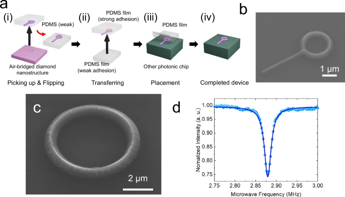
abstract = {Point defects in diamond, particularly nitrogen-vacancy (NV) centers, have emerged as powerful tools for a broad range of quantum technologies. These defects are promising candidates for quantum information science, serving as deterministic single-photon sources and solid-state quantum memories. They have also been employed as nanoscale quantum sensors to detect various physical quantities, including magnetic fields, electric fields, and temperature, owing to their long spin coherence time at room temperature. Development of these diamond-based quantum technologies has been rapidly boosted by a recent quantum leap in nanofabrication technologies for high-quality single-crystal diamond. Incorporating these color centers into diamond nanostructures with mature integrated photonics provides a promising route to build scalable and practical systems for quantum applications. This review discusses recent progress and challenges in the hybrid integration of diamond color centers on cutting-edge photonic platforms.},
keywords = {Diamond, Review},
pubstate = {published},
tppubtype = {article}
}
2019
Takashi Yatsui
Recent improvement of silicon absorption in opto-electric devices Journal Article
In: Opto-Electronic Advances, vol. 2, no. 10, pp. 190023, 2019, (review article, selected as cover story).
Abstract | Links | BibTeX | タグ: Direct wave-vector excitation, First, First principle calculation, Indirect band gap, Near-field effect, Plasmon, Review, Si
@article{OEA_RefItem:1,

title = {Recent improvement of silicon absorption in opto-electric devices},

author = {Takashi Yatsui},

doi = {10.29026/oea.2019.190023},

year  = {2019},

date = {2019-10-01},

urldate = {2019-10-01},

journal = {Opto-Electronic Advances},

volume = {2},

number = {10},

pages = {190023},

publisher = {OEA},

abstract = {Silicon dominates the contemporary electronic industry. However, being an indirect band-gap material, it is a poor absorber of light, which decreases the efficiency of Si-based photodetectors and photovoltaic devices. This review highlights recent studies performed towards improving the optical absorption of Si. A summary of recent theoretical approaches based on the first principle calculation has been provided. It is followed by an overview of recent experimental approaches including scattering, plasmon, hot electron, and near-field effects. The article concludes with a perspective on the future research direction of Si-based photodetectors and photovoltaic devices.},

note = {review article, selected as cover story},

keywords = {Direct wave-vector excitation, First, First principle calculation, Indirect band gap, Near-field effect, Plasmon, Review, Si},

pubstate = {published},

tppubtype = {article}

}
2017

Takashi Yatsui, Maiku Yamaguchi, Katsuyuki Nobusada
Nano-scale chemical reactions based on non-uniform optical near-fields and their applications Journal Article
In: Progress in Quantum Electronics, vol. 55, pp. 166 - 194, 2017, ISSN: 0079-6727, (review article).
Abstract | Links | BibTeX | タグ: Artificial photosynthesis, First, Near-field etching, Non-uniform optical near field, Photodissociation path with two-step excitation, Review, Selected, SHG
@article{YATSUI2017166,

title = {Nano-scale chemical reactions based on non-uniform optical near-fields and their applications},

author = {Takashi Yatsui and Maiku Yamaguchi and Katsuyuki Nobusada},

doi = {10.1016/j.pquantelec.2017.06.001},

issn = {0079-6727},

year  = {2017},

date = {2017-09-01},

journal = {Progress in Quantum Electronics},

volume = {55},

pages = {166 - 194},

abstract = {Interaction between light and materials is essential in the physics underlying all optical devices, including light emitting devices such as light emitting diodes and lasers, photo-voltaic devices, and photo-synthesis systems. The demand for higher light utilization efficiency is becoming increasingly important for advanced optical devices. This is because, when feature size is smaller than the incident light wavelength, photons cannot couple with devices efficiently. In this paper, we review recent progress regarding a unique phenomenon at the nano scale and its applications. First, we summarize the development of light–matter interactions at the nano-scale. Second, we review recent theoretical works focusing on optical near fields in which unique phenomena arise from non-uniform optical fields. We then review several recent developments based on the near-field effect, including artificial photosynthesis and near-field etching for realization of angstrom-scale fattened surfaces. Finally, we discuss the future outlook for these technologies.},

note = {review article},

keywords = {Artificial photosynthesis, First, Near-field etching, Non-uniform optical near field, Photodissociation path with two-step excitation, Review, Selected, SHG},

pubstate = {published},

tppubtype = {article}

}
2013

Takashi Yatsui, Wataru Nomura, Fabrice Stehlin, Olivier Soppera, Makoto Naruse, Motoichi Ohtsu
Challenge in realizing ultraflat material surfaces Journal Article
In: Beilstein Journal of Nanotechnology, vol. 4, pp. 875-885, 2013, (review article).
Abstract | Links | BibTeX | タグ: First, Nanophotonic fabrication, Near-field etching, Review, Selected
@article{2013yatsuiBJrev,
title = {Challenge in realizing ultraflat material surfaces},
author = {Takashi Yatsui and Wataru Nomura and Fabrice Stehlin and Olivier Soppera and Makoto Naruse and Motoichi Ohtsu},
doi = {10.3762/bjnano.4.99},
year = {2013},
date = {2013-12-01},
journal = {Beilstein Journal of Nanotechnology},
volume = {4},
pages = {875-885},
publisher = {Beilstein-Institut.},
abstract = {The laser-induced damage threshold (LIDT) is widely used as an index for evaluating an optical componentfs resistance to laser light. However, a degradation in the performance of an optical component is also caused by continuous irradiation with laser light having an energy density below the LIDT. Therefore, here we focused on the degradation in performance of an optical component caused by continuous irradiation with femtosecond laser light having a low energy density, i.e.Ultraflat surface substrates are required to achieve an optimal performance of future optical, electronic, or optoelectronic devices for various applications, because such surfaces reduce the scattering loss of photons, electrons, or both at the surfaces and interfaces. In this paper, we review recent progress toward the realization of ultraflat materials surfaces. First, we review the development of surface-flattening techniques. Second, we briefly review the dressed photon-phonon (DPP), a nanometric quasiparticle that describes the coupled state of a photon, an electron, and a multimode-coherent phonon. Then, we review several recent developments based on DPP-photochemical etching and desorption processes, which have resulted in angstrom-scale flat surfaces. To confirm that the superior flatness of these surfaces that originated from the DPP process, we also review a simplified mathematical model that describes the scale-dependent effects of optical near-fields. Finally, we present the future outlook for these technologies.},
note = {review article},
keywords = {First, Nanophotonic fabrication, Near-field etching, Review, Selected},
pubstate = {published},
tppubtype = {article}
}
2008
Motoichi Ohtsu, Tadashi Kawazoe, Takashi Yatsui, Makoto Naruse
Nanophotonics: Application of Dressed Photons to Novel Photonic Devices and Systems Journal Article
In: IEEE Journal on Selected Topics in Quantum Electronics, vol. 14, no. 6, pp. 1404-1417, 2008, (review article).
Abstract | Links | BibTeX | タグ: Nanophotonic fabrication, Near-field effect, Review
@article{2008IEEE,

title = {Nanophotonics: Application of Dressed Photons to Novel Photonic Devices and Systems},

author = {Motoichi Ohtsu and Tadashi Kawazoe and Takashi Yatsui and Makoto Naruse},

doi = {10.1109/JSTQE.2008.918110},

year  = {2008},

date = {2008-11-01},

journal = {IEEE Journal on Selected Topics in Quantum Electronics},

volume = {14},

number = {6},

pages = {1404-1417},

publisher = {IEEE},

abstract = {This paper reviews recent progress in nanophotonics, a novel optical technology proposed by one of the authors (M. Ohtsu). Nanophotonics utilizes the local interaction between nanometric particles via optical near fields. The optical near fields are the elementary surface excitations on nanometric particles, that is, dressed photons that carry the material energy. Of the variety of qualitative innovations in optical technology realized by nanophotonics, this paper focuses on devices and systems. The principles of device operation are reviewed considering the excitation energy transfer via the optical near-field interaction and subsequent dissipation. As representative examples, the principles of a nanophotonic and gate, not gate, and optical nanofountain are described. Experimental results for operating devices using CuCl quantum dots (QDs), InAlAs QDs, and nanorod ZnO double quantum wells are described. Using a systems-perspective approach, the principles of content-addressable memory based on nanophotonic device operations and experimental results are reviewed. The hierarchy of optical near-field interactions is discussed, and its application to a multilayer memory retrieval system is demonstrated.},

note = {review article},

keywords = {Nanophotonic fabrication, Near-field effect, Review},

pubstate = {published},

tppubtype = {article}

}
2006

Tadashi Kawazoe, Takashi Yatsui, Motoichi Ohtsu
Nanophotonics using optical near fields Journal Article
In: Journal of Non-Crystalline Solids, vol. 352, no. 23, pp. 2492 - 2495, 2006, ISSN: 0022-3093, (review article).
Abstract | Links | BibTeX | タグ: Nanocrystals, Non-linear optics, QW, Review
@article{KAWAZOE20062492,

title = {Nanophotonics using optical near fields},

author = {Tadashi Kawazoe and Takashi Yatsui and Motoichi Ohtsu},

doi = {10.1016/j.jnoncrysol.2006.03.023},

issn = {0022-3093},

year  = {2006},

date = {2006-07-01},

journal = {Journal of Non-Crystalline Solids},

volume = {352},

number = {23},

pages = {2492 - 2495},

abstract = {This paper introduces recent successes in nanophotonics utilizing local electromagnetic interactions between a few nanometric elements (i.e., the optical near-field interaction). The sections of this paper review nanophotonic devices, nanofabrication, and systems for operating nanophotonic devices efficiently. Using CuCl quantum dots, the operations of an optical switch measuring 20-nm in size (i.e., a nanophotonic switch) and a nanometric optical condenser, which attracts optical energy into a 10-nm spot (i.e., an optical nano-fountain), were verified experimentally. The power consumption of these devices is only 1/100000 that of conventional electronic devices. A nanodot coupler fabricated from a linear array of closely spaced metallic nanoparticles has also been introduced for transmitting an optical signal to a nanophotonic device. To increase the optical far- to near-field conversion efficiency for transmission, a surface plasmon polariton (SPP) condenser was fabricated from hemispherical metallic nanoparticles, so that it worked as a ‘phased array’. The SPP can be focused with a spot size as small as 400nm.},

note = {review article},

keywords = {Nanocrystals, Non-linear optics, QW, Review},

pubstate = {published},

tppubtype = {article}

}
Haruhiko Ito, Kazuhiro Yamamoto, Akifumi Takamizawa, Hiroyuki Kashiwagi, Takashi Yatsui
Deflecting, focusing, and funnelling atoms by near-field light Journal Article
In: Journal of Optics A: Pure and Applied Optics, vol. 8, no. 4, pp. S153-S160, 2006, (review article).
Abstract | Links | BibTeX | タグ: Atom, Near-field effect, Review
@article{Ito_2006,

title = {Deflecting, focusing, and funnelling atoms by near-field light},

author = {Haruhiko Ito and Kazuhiro Yamamoto and Akifumi Takamizawa and Hiroyuki Kashiwagi and Takashi Yatsui},

doi = {10.1088/1464-4258/8/4/s16},

year  = {2006},

date = {2006-03-01},

journal = {Journal of Optics A: Pure and Applied Optics},

volume = {8},

number = {4},

pages = {S153-S160},

publisher = {IOP Publishing},

abstract = {We describe atom deflection with a slit-type deflector as an elemental

technique of precise atom control using near-field light. In the demonstration

experiments, cold Rb atoms deflected by repulsive near-field light induced in a

200 nm-wide slit are detected by means of two-step photoionization. Then, we

consider a near-field-light lens of atomic de Broglie waves by developing the

atom deflector. The feasibility of nanofocusing is shown by numerical analyses

with Fourier atom optics. Finally, we describe atom funnels with evanescent

light to generate a cold atomic beam required for atom manipulation using

nanometric near-field light. The flux intensity of cold Rb atoms outputted from a

240 µm outlet is estimated

to be 7.5 × 10⁷ atom cm−2 s−1 at a blue

detuning of 1.2 GHz. In order to increase the flux intensity to

1012 atom cm−2 s−1, we develop a Si-made funnel with a micron-sized outlet.},

note = {review article},

keywords = {Atom, Near-field effect, Review},

pubstate = {published},

tppubtype = {article}

}
technique of precise atom control using near-field light. In the demonstration
experiments, cold Rb atoms deflected by repulsive near-field light induced in a
200 nm-wide slit are detected by means of two-step photoionization. Then, we
consider a near-field-light lens of atomic de Broglie waves by developing the
atom deflector. The feasibility of nanofocusing is shown by numerical analyses
with Fourier atom optics. Finally, we describe atom funnels with evanescent
light to generate a cold atomic beam required for atom manipulation using
nanometric near-field light. The flux intensity of cold Rb atoms outputted from a
240 µm outlet is estimated
to be 7.5 × 10⁷ atom cm−2 s−1 at a blue
detuning of 1.2 GHz. In order to increase the flux intensity to
1012 atom cm−2 s−1, we develop a Si-made funnel with a micron-sized outlet.
2002
Motoichi Ohtsu, Kiyoshi Kobayashi, Tadashi Kawazoe, Suguru Sangu, Takashi Yatsui
Nanophotonics: design, fabrication, and operation of nanometric devices using optical near fields Journal Article
In: IEEE Journal of Selected Topics in Quantum Electronics, vol. 8, no. 4, pp. 839-862, 2002, (review article).
Abstract | Links | BibTeX | タグ: Nanophotonic device, Nanophotonic fabrication, Review, Selected
@article{2008IEEEb,

title = {Nanophotonics: design, fabrication, and operation of nanometric devices using optical near fields},

author = {Motoichi Ohtsu and Kiyoshi Kobayashi and Tadashi Kawazoe and Suguru Sangu and Takashi Yatsui},

doi = {10.1109/JSTQE.2002.801738},

year  = {2002},

date = {2002-07-01},

journal = {IEEE Journal of Selected Topics in Quantum Electronics},

volume = {8},

number = {4},

pages = {839-862},

publisher = {IEEE},

abstract = {This paper reviews progress in nanophotonics, a novel optical nanotechnology, utilizing local electromagnetic interactions between a few nanometric elements and an optical near field. A prototype of a nanophotonic integrated circuit (IC) is presented, in which the optical near field is used as a carrier to transmit a signal from one nanometric dot to another. Each section of this paper reviews theoretical and experimental studies carried out to assess the possibility of designing, fabricating, and operating each nanophotonic IC device. A key device, the nanophotonic switch, is proposed based on optical near-field energy transfer between quantum dots (QDs). The optical near-field interaction is expressed as the sum of the Yukawa function, and the oscillation period of the nutation of cubic CuCl QDs is estimated to be less than 100 ps. To guarantee one-directional (i.e., irreversible) energy transfer between two resonant levels of QDs, intrasublevel transitions due to phonon coupling are examined by considering a simple two-QD plus phonon heat bath system. As a result, the state-filling time is estimated as 22 ps for CuCl QDs. This time is almost independent of the temperature in the Born-Markov approximation. Using cubic CuCl QDs in a NaCl matrix as a test sample, the optical near-field energy transfer was experimentally verified by near-field optical spectroscopy with a spatial resolution smaller than 50 nm in the near-UV region at 15 K. This transfer occurs from the lowest state of excitons in 4.6-nm QDs to the first dipole-forbidden excited state of excitons in 6.3-nm QDs. To fabricate nanophotonic devices and ICs, chemical vapor deposition using an optical near field is proposed; this is sufficiently precise in controlling the size and position of the deposited material. A novel deposition scheme under nonresonant conditions is also demonstrated and its origin is discussed. In order to confirm the possibility of using a nanometric ZnO dot as a light emitter in a nanophotonic IC, spatially and spectrally resolved photoluminescence imaging of individual ZnO nanocrystallites was carried out with a spatial resolution as high as 55 nm, using a UV fiber probe, and the spectral shift due to the quantum size effect was found. To connect the nanophotonic IC to external photonic devices, a nanometer-scale waveguide was developed using a metal-coated silicon wedge structure. Illumination (wavelength: 830 nm) of the metal-coated silicon wedge (width: 150 nm) excites a TM plasmon mode with a beam width of 150 nm and propagation length of 2.5 /spl mu/m. A key device for nanophotonics, an optical near-field probe with an extremely high throughput, was developed by introducing a pyramidal silicon structure with localized surface plasmon resonance at the metallized probe tip. A throughput as high as 2.3% was achieved. Finally, as an application of nanophotonics to, a high-density, high-speed optical memory system, a novel contact slider with a pyramidal silicon probe array was developed. This slider was used for phase-change recording and reading, and a mark length as short as 110 nm was demonstrated.},

note = {review article},

keywords = {Nanophotonic device, Nanophotonic fabrication, Review, Selected},

pubstate = {published},

tppubtype = {article}

}