Publications
ResearcherID : C-5956-2008 (TY, h-index: 25) , AAZ-8749-2021 (RK, h-index: 13)
Google Scholar : TY (h-index: 35), RK (h-index: 14), KT (h-index: 4)
Research Square: TY
2020

Sarath Raman Nair, Lachlan J. Rogers, Xavier Vidal, Reece P. Roberts, Hiroshi Abe, Takeshi Ohshima, Takashi Yatsui, Andrew D. Greentree, Jan Jeske, Thomas Volz
Amplification by stimulated emission of nitrogen-vacancy centres in a diamond-loaded fibre cavity Journal Article
In: Nanophotonics, vol. 9, no. 15, pp. 4505-4518, 2020.
Abstract | Links | BibTeX | タグ: Near-field etching, NV center
@article{amp20,

title = {Amplification by stimulated emission of nitrogen-vacancy centres in a diamond-loaded fibre cavity},

author = {Sarath Raman Nair and Lachlan J. Rogers and Xavier Vidal and Reece P. Roberts and Hiroshi Abe and Takeshi Ohshima and Takashi Yatsui and Andrew D. Greentree and Jan Jeske and Thomas Volz},

doi = {10.1515/nanoph-2020-0305},

year  = {2020},

date = {2020-11-01},

urldate = {2020-11-01},

journal = {Nanophotonics},

volume = {9},

number = {15},

pages = {4505-4518},

abstract = {Laser threshold magnetometry using the negatively charged nitrogen-vacancy (NV−) centre in diamond as a gain medium has been proposed as a technique to dramatically enhance the sensitivity of room-temperature magnetometry. We experimentally explore a diamond-loaded open tunable fibre-cavity system as a potential contender for the realisation of lasing with NV− centres. We observe amplification of the transmission of a cavity-resonant seed laser at 721 nm when the cavity is pumped at 532 nm and attribute this to stimulated emission. Changes in the intensity of spontaneously emitted photons accompany the amplification, and a qualitative model including stimulated emission and ionisation dynamics of the NV− centre captures the dynamics in the experiment very well. These results highlight important considerations in the realisation of an NV− laser in diamond.},

keywords = {Near-field etching, NV center},

pubstate = {published},

tppubtype = {article}

}
2018
Felix Brandenburg, Ryosuke Nagumo, Kota Saichi, Kosuke Tahara, Takayuki Iwasaki, Mutsuko Hatano, Fedor Jelezko, Ryuji Igarashi, Takashi Yatsui
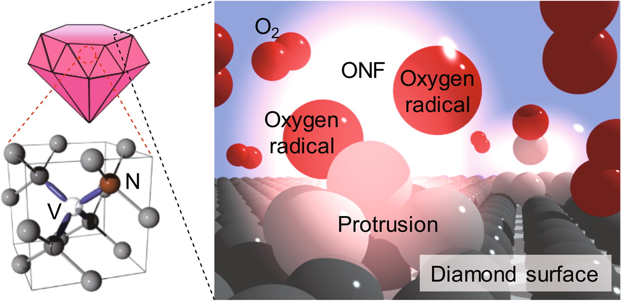
Improving the electron spin properties of nitrogen-vacancy centres in nanodiamonds by near-field etching Journal Article
In: Scientific Reports, vol. 8, pp. 15847, 2018.
Abstract | Links | BibTeX | タグ: Diamond, Nanophotonic fabrication, Near-field etching, NV center
@article{2018Felix,

title = {Improving the electron spin properties of nitrogen-vacancy centres in nanodiamonds by near-field etching},

author = {Felix Brandenburg and Ryosuke Nagumo and Kota Saichi and Kosuke Tahara and Takayuki Iwasaki and Mutsuko Hatano and Fedor Jelezko and Ryuji Igarashi and Takashi Yatsui},

doi = {10.1038/s41598-018-34158-4},

year  = {2018},

date = {2018-10-01},

urldate = {2018-10-01},

journal = {Scientific Reports},

volume = {8},

pages = {15847},

publisher = {Springer Nature},

abstract = {The nitrogen-vacancy (NV) centre in diamond is a promising candidate for quantum computing applications and magnetic sensing applications, because it is an atomic-scale defect with stable coherence time (T2) and reliable accessibility at room temperature. We demonstrated a method for improving the NV spin properties (the full width half maximum (FWHM) value of the magnetic resonance spectrum and T2) through a near-field (NF) etching method under ambient conditions. The NF etching method, based on a He-Cd ultraviolet laser (325 nm), which is longer than the absorption edge of the oxygen molecule, enabled selective removal of defects on the nanodiamond surface. We observed a decrease in the FWHM value close to 15% and an increase in T2 close to 25%. Since our technique can be easily reproduced, a wide range of NV centre applications could be improved, especially magnetic sensing applications. Our results are especially attractive, because they have been obtained under ambient conditions and only require a light source with wavelength slightly above the O2 absorption edge.},

keywords = {Diamond, Nanophotonic fabrication, Near-field etching, NV center},

pubstate = {published},

tppubtype = {article}

}
2017
Takashi Yatsui, Hiroshi Saito, Katsuhiro Nishioka, Benjamin Leuschel, Olivier Soppera, Katsuyuki Nobusada
Effects of a power and photon energy of incident light on near-field etching properties Journal Article
In: Applied Physics A, vol. 123, no. 12, pp. 751, 2017.
Abstract | Links | BibTeX | タグ: First, Nanophotonic fabrication, Near-field etching
@article{2017yatsuiAPA,

title = {Effects of a power and photon energy of incident light on near-field etching properties},

author = {Takashi Yatsui and Hiroshi Saito and Katsuhiro Nishioka and Benjamin Leuschel and Olivier Soppera and Katsuyuki Nobusada},

doi = {10.1007/s00339-017-1361-z},

year  = {2017},

date = {2017-12-01},

journal = {Applied Physics A},

volume = {123},

number = {12},

pages = {751},

publisher = {Springer Nature},

abstract = {We developed a near-field etching technique for realizing an ultra-flat surfaces of various materials and structures. To elucidate the near-field etching properties, we have investigated the effects of power and the photon energy of the incident light. First, we established theoretically that an optical near-field with photon energy lower than the absorption edge of the molecules can induce molecular vibrations. We used nanodiamonds to study the power dependence of the near-field etching properties. From the topological changes of the nanodiamonds, we confirmed the linear-dependence of the etching volume with the incident power. Furthermore, we studied the photon energy dependence using TiO2 nanostriped structures, which revealed that a lower photon energy results in a lower etching rate.},

keywords = {First, Nanophotonic fabrication, Near-field etching},

pubstate = {published},

tppubtype = {article}

}
Takashi Yatsui, Hiroshi Saito, Katsuyuki Nobusada
Angstrom-scale flatness using selective nanoscale etching Journal Article
In: Beilstein Journal of Nanotechnology, vol. 123, pp. 751, 2017.
Abstract | Links | BibTeX | タグ: First, Nanophotonic fabrication, Near-field etching, Wet etching
@article{2017yatsuiBJ,
title = {Angstrom-scale flatness using selective nanoscale etching},
author = {Takashi Yatsui and Hiroshi Saito and Katsuyuki Nobusada},
doi = {10.3762/bjnano.8.217},
year = {2017},
date = {2017-10-01},
journal = {Beilstein Journal of Nanotechnology},
volume = {123},
pages = {751},
publisher = {Beilstein-Institut.},
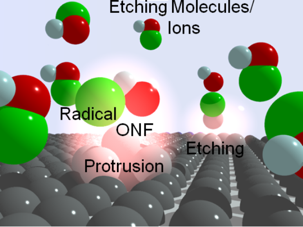
abstract = {The realization of flat surfaces on the angstrom scale is required in advanced devices to avoid loss due to carrier (electron and/or photon) scattering. In this work, we have developed a new surface flattening method that involves near-field etching, where optical near-fields (ONFs) act to dissociate the molecules. ONFs selectively generated at the apex of protrusions on the surface selectively etch the protrusions. To confirm the selective etching of the nanoscale structure, we compared near-field etching using both gas molecules and ions in liquid phase. Using two-dimensional Fourier analysis, we found that near-field etching is an effective way to etch on the scale of less than 10 nm for both wet and dry etching techniques. In addition, near-field dry etching may be effective for the selective etching of nanoscale structures with large mean free path values.},
keywords = {First, Nanophotonic fabrication, Near-field etching, Wet etching},
pubstate = {published},
tppubtype = {article}
}

Takashi Yatsui, Maiku Yamaguchi, Katsuyuki Nobusada
Nano-scale chemical reactions based on non-uniform optical near-fields and their applications Journal Article
In: Progress in Quantum Electronics, vol. 55, pp. 166 - 194, 2017, ISSN: 0079-6727, (review article).
Abstract | Links | BibTeX | タグ: Artificial photosynthesis, First, Near-field etching, Non-uniform optical near field, Photodissociation path with two-step excitation, Review, Selected, SHG
@article{YATSUI2017166,

title = {Nano-scale chemical reactions based on non-uniform optical near-fields and their applications},

author = {Takashi Yatsui and Maiku Yamaguchi and Katsuyuki Nobusada},

doi = {10.1016/j.pquantelec.2017.06.001},

issn = {0079-6727},

year  = {2017},

date = {2017-09-01},

journal = {Progress in Quantum Electronics},

volume = {55},

pages = {166 - 194},

abstract = {Interaction between light and materials is essential in the physics underlying all optical devices, including light emitting devices such as light emitting diodes and lasers, photo-voltaic devices, and photo-synthesis systems. The demand for higher light utilization efficiency is becoming increasingly important for advanced optical devices. This is because, when feature size is smaller than the incident light wavelength, photons cannot couple with devices efficiently. In this paper, we review recent progress regarding a unique phenomenon at the nano scale and its applications. First, we summarize the development of light–matter interactions at the nano-scale. Second, we review recent theoretical works focusing on optical near fields in which unique phenomena arise from non-uniform optical fields. We then review several recent developments based on the near-field effect, including artificial photosynthesis and near-field etching for realization of angstrom-scale fattened surfaces. Finally, we discuss the future outlook for these technologies.},

note = {review article},

keywords = {Artificial photosynthesis, First, Near-field etching, Non-uniform optical near field, Photodissociation path with two-step excitation, Review, Selected, SHG},

pubstate = {published},

tppubtype = {article}

}
Felix Brandenburg, Tomohiro Okamoto, Hiroshi Saito, Benjamin Leuschel, Olivier Soppera, Takashi Yatsui
Surface improvement of organic photoresists using a near-field-dependent etching method Journal Article
In: Beilstein Journal of Nanotechnology, vol. 8, pp. 784-788, 2017.
Abstract | Links | BibTeX | タグ: Nanophotonic fabrication, Near-field etching
@article{2017FelixBJ,

title = {Surface improvement of organic photoresists using a near-field-dependent etching method},

author = {Felix Brandenburg and Tomohiro Okamoto and Hiroshi Saito and Benjamin Leuschel and Olivier Soppera and Takashi Yatsui},

doi = {10.3762/bjnano.8.81},

year  = {2017},

date = {2017-04-01},

journal = {Beilstein Journal of Nanotechnology},

volume = {8},

pages = {784-788},

publisher = {Beilstein-Institut.},

abstract = {Surface flattening techniques are extremely important for the development of future electrical and/or optical devices because carrier-scattering losses due to surface roughness severely limit the performance of nanoscale devices. To address the problem, we have developed a near-field etching technique that provides selective etching of surface protrusions, resulting in an atomically flat surface. To achieve finer control, we examine the importance of the wavelength of the near-field etching laser. Using light sources at wavelengths of 325 and 405 nm, which are beyond the absorption edge of the photoresist (310 nm), we compare the resulting cross-sectional etching volumes. The volumes were larger when 325 nm light was employed, i.e., closer to the absorption edge. Although 405 nm light did not cause structural change in the photoresist, a higher reduction of the surface roughness was observed as compared to the 325 nm light. These results indicate that even wavelengths above 325 nm can cause surface roughness improvements without notably changing the structure of the photoresist.},

keywords = {Nanophotonic fabrication, Near-field etching},

pubstate = {published},

tppubtype = {article}

}
2016
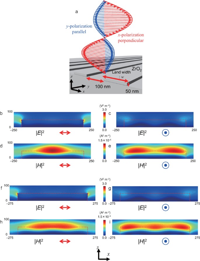
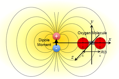
Takashi Yatsui, Toshiki Tsuboi, Maiku Yamaguchi, Katsuyuki Nobusada, Satoshi Tojo, Fabrice Stehlin, Olivier Soppera, Daniel Bloch
Optically controlled magnetic-field etching on the nano-scale Journal Article
In: Light: Science & Applications, vol. 5, pp. e16054, 2016.
Abstract | Links | BibTeX | タグ: First, Nanophotonic fabrication, Near-field etching, Selected
@article{2016YatsuiLST,

title = {Optically controlled magnetic-field etching on the nano-scale},

author = {Takashi Yatsui and Toshiki Tsuboi and Maiku Yamaguchi and Katsuyuki Nobusada and Satoshi Tojo and Fabrice Stehlin and Olivier Soppera and Daniel Bloch},

url = {https://www.altmetric.com/details/6399772},

doi = {10.1038/lsa.2016.54},

year  = {2016},

date = {2016-03-25},

journal = {Light: Science & Applications},

volume = {5},

pages = {e16054},

publisher = {Springer Nature},

abstract = {Electric and magnetic fields play an important role in both chemical and physical reactions. However, since the coupling efficiency between magnetic fields and electrons is low in comparison with that between electric fields and electrons in the visible wavelength region, the magnetic field is negligible in photo-induced reactions. Here, we performed photo-etching of ZrO2 nano-stripe structures, and identified an etching-property polarisation dependence. Specifically, the etching rate and etched profiles depend on the structure width. To evaluate this polarisation-dependent etching, we performed numerical calculations using a finite-difference time-domain method. Remarkably, the numerical results revealed that the polarisation-dependent etching properties were determined by the magnetic field distributions, rather than the electric field distributions. As nano-scale structures induce a localised magnetic field, the discovery of this etching dependence on the magnetic field is expected to introduce a new perspective on advanced nano-scale structure fabrication.},

keywords = {First, Nanophotonic fabrication, Near-field etching, Selected},

pubstate = {published},

tppubtype = {article}

}
2015
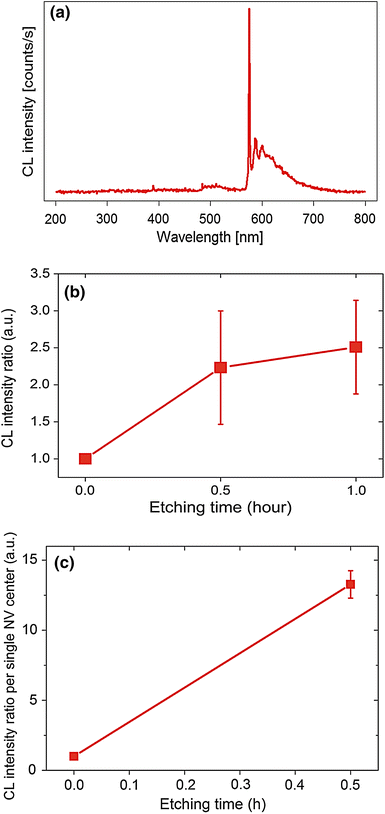
Ryosuke Nagumo, Felix Brandenburg, Anna Ermakova, Fedor Jelezko, Takashi Yatsui
Spectral control of nanodiamond using dressed photon-phonon etching Journal Article
In: Applied Physics A, vol. 121, no. 4, pp. 1335-1339, 2015.
Abstract | Links | BibTeX | タグ: Diamond, Nanophotonic fabrication, Near-field etching, NV center
@article{2015NagumoAPA,

title = {Spectral control of nanodiamond using dressed photon-phonon etching},

author = {Ryosuke Nagumo and Felix Brandenburg and Anna Ermakova and Fedor Jelezko and Takashi Yatsui},

doi = {10.1007/s00339-015-9400-0},

year  = {2015},

date = {2015-12-01},

journal = {Applied Physics A},

volume = {121},

number = {4},

pages = {1335-1339},

publisher = {Springer Nature},

abstract = {The luminescence of a nitrogen-vacancy (NV) center in a nanodiamond (ND) is of great interest because of its features, especially in the field of nanophotonics. When an NV center in an ND is located in the vicinity of the surface, the emission is often disturbed by any surface defects, resulting in non-radiative recombination. In this work, we performed dressed photon-phonon (DPP) etching of the NDs, and found that the size of the NDs decreased, while the cathodoluminescence (CL) intensity increased. We assume that this increase in the CL intensity originates from the removal of the surface protrusions and/or defects by DPP etching.},

keywords = {Diamond, Nanophotonic fabrication, Near-field etching, NV center},

pubstate = {published},

tppubtype = {article}

}
Wataru Nomura, Takashi Yatsui, Tadashi Kawazoe, Naoya Tate, Motoichi Ohtsu
High-speed flattening of crystallized glass substrates by dressed-photon-phonon etching Journal Article
In: Applied Physics A, vol. 121, no. 4, pp. 1403-1407, 2015.
Abstract | Links | BibTeX | タグ: Nanophotonic fabrication, Near-field etching
@article{2015NomuraAPA,
title = {High-speed flattening of crystallized glass substrates by dressed-photon-phonon etching},
author = {Wataru Nomura and Takashi Yatsui and Tadashi Kawazoe and Naoya Tate and Motoichi Ohtsu},
doi = {10.1007/s00339-015-9466-8},
year = {2015},
date = {2015-12-01},
journal = {Applied Physics A},
volume = {121},
number = {4},
pages = {1403-1407},
publisher = {Springer Nature},
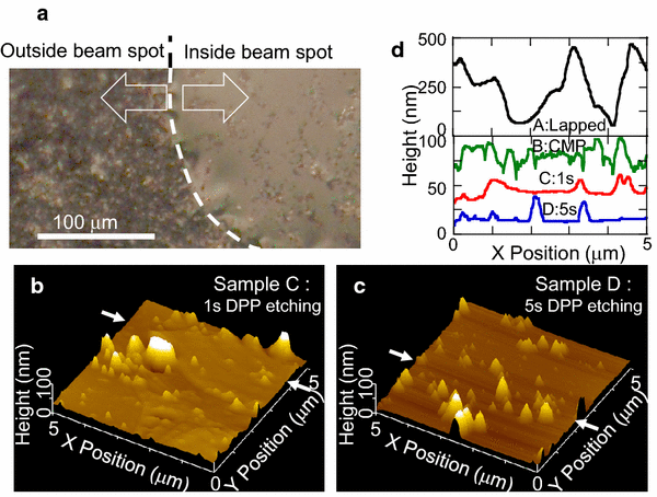
abstract = {Dressed-photon-phonon (DPP) etching is a non-contact flattening technology that realizes ultra-flat surfaces and has been reported to achieve an arithmetic mean surface roughness, R a, on the order of 0.1 nm in various materials, such as fused silica, plastic films, and GaN crystal. In this study, we successfully flattened the surface of a crystallized glass substrate in several seconds using laser light with a higher power density than that used in previous studies. The target substrate had an initial appearance similar to frosted glass, with an R a of 92.5 nm. We performed DPP etching under a Cl2 atmosphere using a CW laser with a wavelength of 532 nm, a power of 8 W, and a spot diameter of 0.2 mm. After 1 s of processing, we obtained a flat surface with an R a of 5.00 nm. This surface roughness equaled or surpassed that of a substrate flattened by conventional chemical mechanical polishing, with an R a of 5.77 nm. Through the detailed analysis of atomic force microscopic images, we found the DPP etching resulted in the smaller standard deviation of the height difference than CMP in the smaller lateral size than 50 nm.},
keywords = {Nanophotonic fabrication, Near-field etching},
pubstate = {published},
tppubtype = {article}
}

Takashi Yatsui, Wataru Nomura, Motoichi Ohtsu
Realization of Ultraflat Plastic Film Using Dressed-Photon-Phonon-Assisted Selective Etching of Nanoscale Structures Journal Article
In: Advances in Optical Technologies, vol. 2015, pp. 701802, 2015.
Abstract | Links | BibTeX | タグ: First, Nanophotonic fabrication, Near-field etching
@article{2015Plastic,

title = {Realization of Ultraflat Plastic Film Using Dressed-Photon-Phonon-Assisted Selective Etching of Nanoscale Structures},

author = {Takashi Yatsui and Wataru Nomura and Motoichi Ohtsu},

doi = {10.1155/2015/701802},

year  = {2015},

date = {2015-02-01},

urldate = {2015-02-01},

journal = {Advances in Optical Technologies},

volume = {2015},

pages = {701802},

abstract = {We compared dressed-photon-phonon (DPP) etching to conventional photochemical etching and, using a numerical analysis of topographic images of the resultant etched polymethyl methacrylate (PMMA) substrate, we determined that the DPP etching resulted in the selective etching of smaller scale structures in comparison with the conventional photochemical etching. We investigated the wavelength dependence of the PMMA substrate etching using an O2 gas. As the dissociation energy of O2 is 5.12 eV, we applied a continuous-wave (CW) He-Cd laser ( 325 nm, 3.81 eV) for the DPP etching and a 5th-harmonic Nd:YAG laser (213  nm, 5.82 eV) for the conventional photochemical etching. From the obtained atomic force microscope images, we confirmed a reduction in surface roughness, Ra, in both cases. However, based on calculations involving the standard deviation of the height difference function, we confirmed that the conventional photochemical etching method etched the larger scale structures only, while the DPP etching process selectively etched the smaller scale features.},

keywords = {First, Nanophotonic fabrication, Near-field etching},

pubstate = {published},

tppubtype = {article}

}
2014

Takashi Yatsui, Daisuke Takeuchi, Satoshi Koizumi, Kazuki Sato, Kohei Tsuzuki, Takayuki Iwasaki, Mutsuko Hatano, Toshiharu Makino, Masahiko Ogura, Hiromitsu Kato, Hideyo Okushi, Satoshi Yamasaki
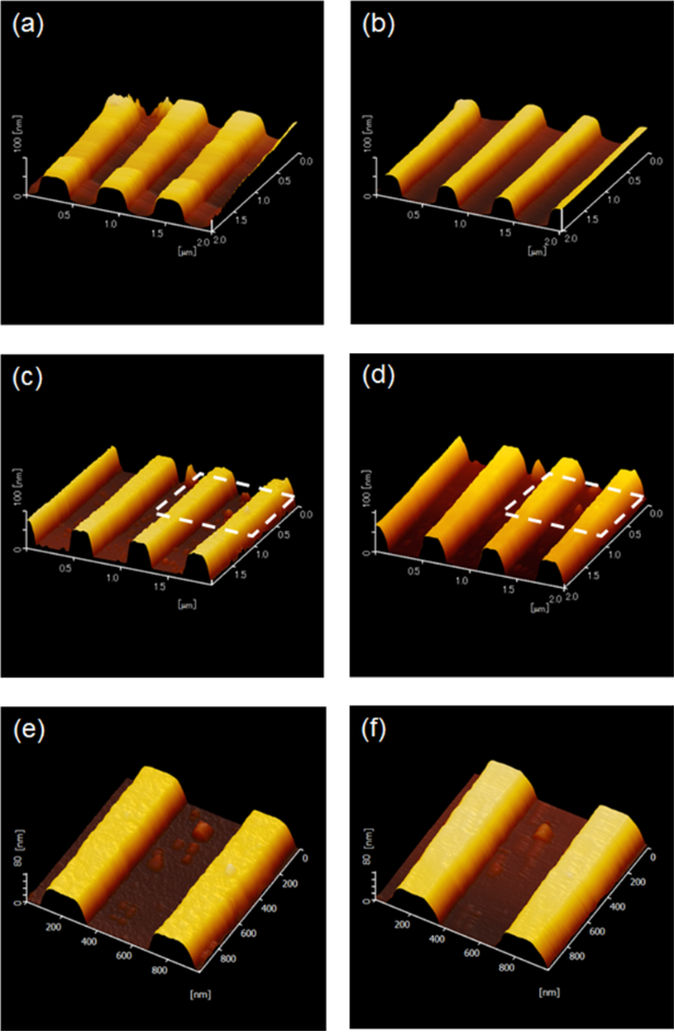
Polarization-controlled dressed-photon–phonon etching of patterned diamond structures Journal Article
In: physica status solidi (a), vol. 211, no. 10, pp. 2339-2342, 2014.
Abstract | Links | BibTeX | タグ: Diamond, First, Nanophotonic fabrication, Near-field etching
@article{doi:10.1002/pssa.201431161,

title = {Polarization-controlled dressed-photon–phonon etching of patterned diamond structures},

author = {Takashi Yatsui and Daisuke Takeuchi and Satoshi Koizumi and Kazuki Sato and Kohei Tsuzuki and Takayuki Iwasaki and Mutsuko Hatano and Toshiharu Makino and Masahiko Ogura and Hiromitsu Kato and Hideyo Okushi and Satoshi Yamasaki},

doi = {10.1002/pssa.201431161},

year  = {2014},

date = {2014-10-01},

journal = {physica status solidi (a)},

volume = {211},

number = {10},

pages = {2339-2342},

abstract = {To realize an ultra-flat diamond surface with a three-dimensional (3D) structure, we performed dressed-photon–phonon (DPP) etching. A DPP is generated on nano-scale protrusions. Hence, the generation of DPPs results in selective removal of nano-scale protrusions, thereby achieving an ultra-flat surface even on the sidewall of a diamond mesa structure. By controlling the polarization of the incident light, a smooth diamond mesa structure sidewall was obtained, and a higher etching rate was obtained with a perpendicular polarization on the corrugations. In addition, by selective deposition of n-layer diamond on the p-layer diamond mesa structure, smooth n-layer diamond was confirmed on the DPP etched sidewall. Schematic of dressed-photon–phonon (DPP) etching on the sidewall: (a) before and (b) after etching, in which DPP selectively generates on the corrugations and etching automatically stops when the surface was smooth. Scanning electron microscopy image of the selective deposition of the n-layer (c) without and (d) with the DPP etched sidewall.},

keywords = {Diamond, First, Nanophotonic fabrication, Near-field etching},

pubstate = {published},

tppubtype = {article}

}
Wataru Nomura, Tadashi Kawazoe, Takashi Yatsui, Makoto Naruse, Motoichi Ohtsu
In: Beilstein Journal of Nanotechnology, vol. 5, pp. 1334-1340, 2014.
Abstract | Links | BibTeX | タグ: Nanophotonic fabrication, Near-field etching
@article{2014ZAISBJb,
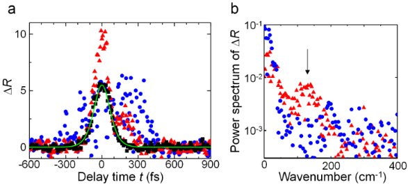
title = {Observation and analysis of structural changes in fused silica by continuous irradiation with femtosecond laser light having an energy density below the laser-induced damage threshold},
author = {Wataru Nomura and Tadashi Kawazoe and Takashi Yatsui and Makoto Naruse and Motoichi Ohtsu},
doi = {10.3762/bjnano.5.146},
year = {2014},
date = {2014-08-01},
journal = {Beilstein Journal of Nanotechnology},
volume = {5},
pages = {1334-1340},
publisher = {Beilstein-Institut.},
abstract = {The laser-induced damage threshold (LIDT) is widely used as an index for evaluating an optical componentfs resistance to laser light. However, a degradation in the performance of an optical component is also caused by continuous irradiation with laser light having an energy density below the LIDT. Therefore, here we focused on the degradation in performance of an optical component caused by continuous irradiation with femtosecond laser light having a low energy density, i.e., laser-induced degradation. We performed an in situ observation and analysis of an increase in scattering light intensity in fused silica substrates. In experiments conducted using a pulsed laser with a wavelength of 800 nm, a pulse width of 160 fs and pulse repetition rate of 1 kHz, we found that the scattered light intensity increased starting from a specific accumulated fluence, namely, that the laser-induced degradation had a threshold. We evaluated the threshold fluence Ft as 6.27 J/cm2 and 9.21 J/cm2 for the fused silica substrates with surface roughnesses of 0.20 nm and 0.13 nm in Ra value, respectively, showing that the threshold decreased as the surface roughness increased. In addition, we found that the reflected light spectrum changed as degradation proceeded. We analyzed the details of the degradation by measuring instantaneous reflectance changes with a pump-probe method; we observed an increase in the generation probability of photogenerated carriers in a degraded silica substrate and a damaged silica substrate and observed a Raman signal originating from a specific molecular structure of silica. From these findings, we concluded that compositional changes in the molecular structure occurred during degradation due to femtosecond laser irradiation having an energy density below the LIDT.},
keywords = {Nanophotonic fabrication, Near-field etching},
pubstate = {published},
tppubtype = {article}
}
2013

Takashi Yatsui, Wataru Nomura, Fabrice Stehlin, Olivier Soppera, Makoto Naruse, Motoichi Ohtsu
Challenge in realizing ultraflat material surfaces Journal Article
In: Beilstein Journal of Nanotechnology, vol. 4, pp. 875-885, 2013, (review article).
Abstract | Links | BibTeX | タグ: First, Nanophotonic fabrication, Near-field etching, Review, Selected
@article{2013yatsuiBJrev,
title = {Challenge in realizing ultraflat material surfaces},
author = {Takashi Yatsui and Wataru Nomura and Fabrice Stehlin and Olivier Soppera and Makoto Naruse and Motoichi Ohtsu},
doi = {10.3762/bjnano.4.99},
year = {2013},
date = {2013-12-01},
journal = {Beilstein Journal of Nanotechnology},
volume = {4},
pages = {875-885},
publisher = {Beilstein-Institut.},
abstract = {The laser-induced damage threshold (LIDT) is widely used as an index for evaluating an optical componentfs resistance to laser light. However, a degradation in the performance of an optical component is also caused by continuous irradiation with laser light having an energy density below the LIDT. Therefore, here we focused on the degradation in performance of an optical component caused by continuous irradiation with femtosecond laser light having a low energy density, i.e.Ultraflat surface substrates are required to achieve an optimal performance of future optical, electronic, or optoelectronic devices for various applications, because such surfaces reduce the scattering loss of photons, electrons, or both at the surfaces and interfaces. In this paper, we review recent progress toward the realization of ultraflat materials surfaces. First, we review the development of surface-flattening techniques. Second, we briefly review the dressed photon-phonon (DPP), a nanometric quasiparticle that describes the coupled state of a photon, an electron, and a multimode-coherent phonon. Then, we review several recent developments based on DPP-photochemical etching and desorption processes, which have resulted in angstrom-scale flat surfaces. To confirm that the superior flatness of these surfaces that originated from the DPP process, we also review a simplified mathematical model that describes the scale-dependent effects of optical near-fields. Finally, we present the future outlook for these technologies.},
note = {review article},
keywords = {First, Nanophotonic fabrication, Near-field etching, Review, Selected},
pubstate = {published},
tppubtype = {article}
}

Makoto Naruse, Takashi Yatsui, Wataru Nomura, Tadashi Kawazoe, Masaki Aida, Motoichi Ohtsu
Unveiling the mechanisms of dressed-photon phonon etching based on hierarchical surface roughness measure Journal Article
In: Applied Physics Letters, vol. 102, no. 7, pp. 071603, 2013.
Abstract | Links | BibTeX | タグ: Near-field etching
@article{doi:10.1063/1.4793233,

title = {Unveiling the mechanisms of dressed-photon phonon etching based on hierarchical surface roughness measure},

author = {Makoto Naruse and Takashi Yatsui and Wataru Nomura and Tadashi Kawazoe and Masaki Aida and Motoichi Ohtsu},

doi = {10.1063/1.4793233},

year  = {2013},

date = {2013-02-01},

urldate = {2013-02-01},

journal = {Applied Physics Letters},

volume = {102},

number = {7},

pages = {071603},

abstract = {Dressed-photon–phonon (DPP) etching is a disruptive technology in planarizing material surfaces because it completely eliminates mechanical contact processes. However, adequate metrics for evaluating the surface roughness and the underlying physical mechanisms are still not well understood. Here, we propose a two-dimensional hierarchical surface roughness measure, inspired by the Allan variance, that represents the effectiveness of DPP etching while conserving the original two-dimensional surface topology. Also, we build a simple physical model of DPP etching that agrees well with the experimental observations, which clearly shows the involvement of the intrinsic hierarchical properties of dressed photons, or optical near-fields, in the surface processing.},

keywords = {Near-field etching},

pubstate = {published},

tppubtype = {article}

}
2012
Takashi Yatsui, Wataru Nomura, Makoto Naruse, Motoichi Ohtsu
Realization of an atomically flat surface of diamond using dressed photon–phonon etching Journal Article
In: Journal of Physics D: Applied Physics, vol. 45, no. 47, pp. 475302, 2012.
Abstract | Links | BibTeX | タグ: Diamond, First, Nanophotonic fabrication, Near-field etching
@article{Yatsui_2012,

title = {Realization of an atomically flat surface of diamond using dressed photon–phonon etching},

author = {Takashi Yatsui and Wataru Nomura and Makoto Naruse and Motoichi Ohtsu},

url = {https://doi.org/10.1088%2F0022-3727%2F45%2F47%2F475302},

doi = {10.1088/0022-3727/45/47/475302},

year  = {2012},

date = {2012-11-01},

journal = {Journal of Physics D: Applied Physics},

volume = {45},

number = {47},

pages = {475302},

publisher = {IOP Publishing},

abstract = {We obtained an atomically flat diamond surface following dressed photon–phonon (DPP) etching using 3.81 eV light and O2 gas. We obtained a surface roughness (Ra) of 0.154 nm for Ib-type (1 1 1) diamond and 0.096 nm for Ib-type (1 0 0) diamond. To evaluate the surface roughness, we grouped the surface into bins of width l and introduced the standard deviation of the height difference function for a given separation l, which allowed us to determine the height variation of the surface. Based on the calculation of standard deviation, the conventional adiabatic photochemical reaction did not remove the small surface features, while DPP etching decreased the surface roughness for all length scales.},

keywords = {Diamond, First, Nanophotonic fabrication, Near-field etching},

pubstate = {published},

tppubtype = {article}

}
2011
Takashi Yatsui, Kazuya Hirata, Yoshinori Tabata, Yumiko Miyake, Yasuyuki Akita, Mamoru Yoshimoto, Wataru Nomura, Tadashi Kawazoe, Makoto Naruse, Motoichi Ohtsu
Self-organized near-field etching of the sidewalls of glass corrugations Journal Article
In: Applied Physics B, vol. 103, no. 3, pp. 527-530, 2011.
Abstract | Links | BibTeX | タグ: First, Nanophotonic fabrication, Near-field etching
@article{2011yatsuiAPBNFE,

title = {Self-organized near-field etching of the sidewalls of glass corrugations},

author = {Takashi Yatsui and Kazuya Hirata and Yoshinori Tabata and Yumiko Miyake and Yasuyuki Akita and Mamoru Yoshimoto and Wataru Nomura and Tadashi Kawazoe and Makoto Naruse and Motoichi Ohtsu},

doi = {10.1007/s00340-011-4569-1},

year  = {2011},

date = {2011-06-01},

journal = {Applied Physics B},

volume = {103},

number = {3},

pages = {527-530},

publisher = {Springer Nature},

abstract = {Using soda-lime glass with a nano-stripe pattern as a test specimen, we demonstrated self-organized near-field etching with a continuum-wave laser (wavelength of 532 nm) light source. Atomic force microscopy confirmed that near-field etching decreases the flank roughness of the corrugations as well as the roughness of the flat surface.},

keywords = {First, Nanophotonic fabrication, Near-field etching},

pubstate = {published},

tppubtype = {article}

}
2010
Takashi Yatsui, Kazuya Hirata, Yoshinori Tabata, Wataru Nomura, Tadashi Kawazoe, Makoto Naruse, Motoichi Ohtsu
In situ real-time monitoring of changes in the surface roughness during nonadiabatic optical near-field etching Journal Article
In: Nanotechnology, vol. 21, no. 35, pp. 355303, 2010.
Abstract | Links | BibTeX | タグ: First, Nanophotonic fabrication, Near-field etching
@article{Yatsuii_2010,

title = {In situ real-time monitoring of changes in the surface roughness during nonadiabatic optical near-field etching},

author = {Takashi Yatsui and Kazuya Hirata and Yoshinori Tabata and Wataru Nomura and Tadashi Kawazoe and Makoto Naruse and Motoichi Ohtsu},

doi = {10.1088/0957-4484/21/35/355303},

year  = {2010},

date = {2010-08-01},

journal = {Nanotechnology},

volume = {21},

number = {35},

pages = {355303},

publisher = {IOP Publishing},

abstract = {We performed in situ real-time monitoring of the change in surface roughness during

self-organized optical near-field etching. During near-field etching of a silica substrate, we detected the scattered light intensity from a continuum wave (CW) laser (λ = 633 nm) in addition to the etching CW laser (λ = 532 nm) light source. We discovered that near-field etching not only decreases surface

roughness, but also increases the number of scatterers, as was confirmed by analyzing the

AFM image. These approaches provide optimization criteria for the etching parameter and

hence for further decreases in surface roughness.},

keywords = {First, Nanophotonic fabrication, Near-field etching},

pubstate = {published},

tppubtype = {article}

}
self-organized optical near-field etching. During near-field etching of a silica substrate, we detected the scattered light intensity from a continuum wave (CW) laser (λ = 633 nm) in addition to the etching CW laser (λ = 532 nm) light source. We discovered that near-field etching not only decreases surface
roughness, but also increases the number of scatterers, as was confirmed by analyzing the
AFM image. These approaches provide optimization criteria for the etching parameter and
hence for further decreases in surface roughness.
2009

Makoto Naruse, Takashi Yatsui, Wataru Nomura, Kazuya Hirata, Yoshinori Tabata, Motoichi Ohtsu
Analysis of surface roughness of optical elements planarized by nonadiabatic optical near-field etching Journal Article
In: Journal of Applied Physics, vol. 105, no. 6, pp. 063516, 2009.
Abstract | Links | BibTeX | タグ: Near-field etching
@article{doi:10.1063/1.3095467,

title = {Analysis of surface roughness of optical elements planarized by nonadiabatic optical near-field etching},

author = {Makoto Naruse and Takashi Yatsui and Wataru Nomura and Kazuya Hirata and Yoshinori Tabata and Motoichi Ohtsu},

url = {https://doi.org/10.1063/1.3095467},

doi = {10.1063/1.3095467},

year  = {2009},

date = {2009-03-01},

urldate = {2009-03-01},

journal = {Journal of Applied Physics},

volume = {105},

number = {6},

pages = {063516},

abstract = {Nonadiabatic optical near-field etching is a novel way of polishing surfaces of optical elements without any mechanical contact processes. It selectively induces photochemical reactions on the surface in regions where optical near fields are excited, namely, in the vicinity of portions having fine-scale rough structures, which leads to reduced surface roughness. In this paper, we analyze the surface roughness of optical elements planarized by nonadiabatic optical near-field etching based on power spectrum-based methods. Our analysis clearly reveals the effects of the near-field etching which are otherwise concealed when using conventional roughness measures such as the roughness average (Ra). We also investigate the effect of planarization via numerical simulations using surface profiles obtained experimentally before and after the near-field etching.},

keywords = {Near-field etching},

pubstate = {published},

tppubtype = {article}

}
2008
Takashi Yatsui, Kazuya Hirata, Wataru Nomura, Yoshinori Tabata, Motoichi Ohtsu
Realization of an ultra-flat silica surface with angstrom-scale average roughness using nonadiabatic optical near-field etching Journal Article
In: Applied Physics B, vol. 93, no. 1, pp. 55-57, 2008.
Abstract | Links | BibTeX | タグ: First, Nanophotonic fabrication, Near-field etching, Selected
@article{2008yatsuiAPBNFE,

title = {Realization of an ultra-flat silica surface with angstrom-scale average roughness using nonadiabatic optical near-field etching},

author = {Takashi Yatsui and Kazuya Hirata and Wataru Nomura and Yoshinori Tabata and Motoichi Ohtsu},

doi = {10.1007/s00340-008-3142-z},

year  = {2008},

date = {2008-10-01},

journal = {Applied Physics B},

volume = {93},

number = {1},

pages = {55-57},

publisher = {Springer Nature},

abstract = {We propose a new method of optical near-field etching where a nonadiabatic process is applied to a synthetic silica substrate using a continuum wave laser (λ=532 nm) with a Cl2 gas source. Because the absorption band edge energy of Cl2 is higher than the photon energy of the light source, we preclude the conventional adiabatic photochemical reaction. An optical near field, generated on the nanometrically rough substrate, induces the nonadiabatic chemical reaction to the Cl2 molecules and thereby selectively etches away the roughness, leaving an ultra-flat synthetic silica surface with a minimum average surface roughness R a of 1.37 A.},

keywords = {First, Nanophotonic fabrication, Near-field etching, Selected},

pubstate = {published},

tppubtype = {article}

}