Near-field etching
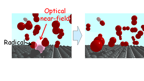
Near-field etching achieve angstrom-scale flat surfaces. Near-field etching is a noncontact method and therefore does not cause damage owing to mechanical polishing, and hence, this technique should help to improve the electrical, optical, and/or electro-optical performance of devices in a variety of applications.
Publications on the near-field etching
- F. Brandenburg, R. Nagumo, K. Saichi, K. Tahara, T. Iwasaki, M. Hatano, F. Jelezko, R. Igarashi, and T. Yatsui, “Improving the electron spin properties of nitrogen-vacancy centres in nanodiamonds by near-field etching,” Scientific Reports, Vol. 8, October 2018, 15847 (8 pages)
- T. Yatsui, H. Saito, K. Nishioka, B. Leuschel, O. Soppera, and K. Nobusada, “Effects of a power and photon energy of incident light on near-field etching properties,” Appl. Phys. A, Volume 123, Issue 12, December 2017, 751
- Takashi Yatsui, Hiroshi Saito, and Katsuyuki Nobusada, “Angstrom-scale flatness using selective nano-scale etching,” Beilstein Journal of Nanotechnology, Vol. 8, October 18, 2017, pp.2181–2185. doi:10.3762/bjnano.8.217.
- T. Yatsui, M. Yamaguchi and K. Nobusada, “Nano-scale chemical reactions based on non-uniform optical near-fields and their applications,” Progress in Quantum Electronics, September 2017, Vol. 55, pp. 166-194, doi: 10.1016/j.pquantelec.2017.06.001. (review article).
- F. J. Brandenburg, T. Okamoto, H. Saito, O. Soppera, and T. Yatsui, “Surface improvement of organic photo-resists through a near-field-dependent etching method,” Beilstein Journal of Nanotechnology, April 2017, Vol. 8, pp.784–788
- T. Yatsui, T. Tsuboi, M. Yamaguchi, K. Nobusada, S. Tojo, F. Stehlin, O. Soppera, and D. Bloch, “Optically controlled magnetic-field etching on the nano-scale,” Light: Science & Applications, Volume 5, March 2016; e16054 (7 pages); doi: 10.1038/lsa.2016.54
- R. Nagumo, F. Brandenburg, A. Ermakova, F. Jelezko, and T. Yatsui, “Spectral control of nanodiamond using dressed photon-phonon etching,” Applied Physics A, Volume 121, Issue 4, December 2015, pp.1335-1339, DOI: 10.1007/s00339-015-9400-0 [invited paper]
- Takashi Yatsui, Wataru Nomura, and Motoichi Ohtsu, “Realization of Ultraflat Plastic Film using Dressed-Photon–Phonon-Assisted Selective Etching of Nanoscale Structures,” Advances in Optical Technologies, February 2015, Article ID 701802 (5 pages)
- T. Yatsui, Daisuke Takeuchi, Satoshi Koizumi, Kazuki Sato, Kohei Tsuzuki, Takayuki Iwasaki, Mutsuko Hatano, Toshiharu Makino Masahiko Ogura, Hiromitsu Kato, Hideyo Okushi, and Satoshi Yamasaki, “Polarization-controlled dressed-photon–phonon etching of patterned diamond structures,” physica status solidi (a), Vol. 211, No. 10, October 2014, pp. 2339–2342, DOI: 10.1002/pssa.201431161
- T. Yatsui, W. Nomura, F. Stehlin, O. Soppera, M. Naruse, and M. Ohtsu, “Challenge in realizing ultraflat material surfaces,” Beilstein Journal of Nanotechnology, December 2013, Volume 4, pp.875–885
- M. Naruse, T. Yatsui, W. Nomura, T. Kawazoe, M. Aida, and M. Ohtsu, “Unveiling the mechanisms of dressed-photon–phonon etching based on hierarchical surface roughness measure,” Appl. Phys. Lett., Vol. 102, No. 7, February 2013, 071603 (5 pages).
- T. Yatsui, W. Nomura, M. Naruse, and M. Ohtsu, “Realization of an atomically flat surface of diamond using dressed-photon phonon etching,” J. Phys. D, Volume 45, Number 47, November 2012, 475302 (4 pages), DOI:10.1088/0022-3727/45/47/475302.
- T. Yatsui, K. Hirata, Y. Tabata, Y. Miyake, Y. Akita, M. Yoshimoto, W. Nomura, T. Kawazoe, M. Naruse, and M. Ohtsu, “Self-organized near-field etching of the sidewalls of glass corrugations,” Appl. Phys. B- Lasers and Optics, Volume 103, Number 3, June 2011, pp.527-530.
- T. Yatsui, K. Hirata, Y. Tabata, W. Nomura, T. Kawazoe, M. Naruse, and M. Ohtsu, “In situ real-time monitoring of changes in the surface roughness during nonadiabatic optical near-field etching,” Nanotechnology, Vol. 21, No. 35, August 2010, 355303 (5 pages)
- N. Tate, H. Sugiyama, M. Naruse, W. Nomura, T. Yatsui, T. Kawazoe, and M. Ohtsu, “Quadrupole-Dipole Transform based on Optical Near-Field Interactions in Engineered Nanostructures,” Opt. Express, Vol. 17, Issue 13, June 2009, pp.11113-11121
- Makoto Naruse, Takashi Yatsui, Wataru Nomura, Kazuya Hirata, Yoshinori Tabata, and Motoichi Ohtsu, “Analysis of surface roughness of optical elements planarized by nonadiabatic optical near-field etching,” J. Appl. Phys. Vol. 105, No. 6, Mar. 2009, 063516 (4 pages)
- T. Yatsui, K. Hirata, W. Nomura, Y. Tabata, and M. Ohtsu, “Realization of an ultra-flat silica surface with angstrom-scale average roughness using nonadiabatic optical near-field etching,” Appl. Phys. B- Lasers and Optics, Vol. 93, No. 1, Oct. 2008, pp.55-57