Articles
back to Achievements
2011
八井崇,
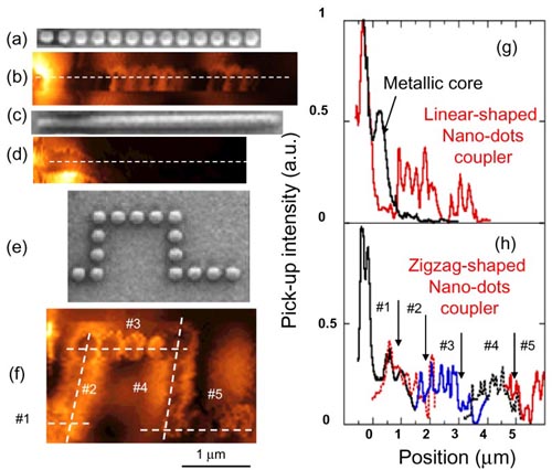
近接場光カップラの進展 Technical Report
2011, (応用物理, Vol. 80, No. 9, pp.790-793).
Links | BibTeX | タグ: Nanophotonic device
@techreport{coupler,

title = {近接場光カップラの進展},

author = {八井崇},

doi = {10.11470/oubutsu.80.9_790},

year  = {2011},

date = {2011-09-01},

urldate = {2011-09-01},

note = {応用物理, Vol. 80, No. 9, pp.790-793},

keywords = {Nanophotonic device},

pubstate = {published},

tppubtype = {techreport}

}
八井崇、大津元一,
ZnOナノ構造のナノフォトニックデバイスへの応用 Technical Report
2011, (レーザー研究,第39巻,第3号,pp.184-187).
Abstract | Links | BibTeX | タグ: Nanophotonic device
@techreport{ZnOdevice,

title = {ZnOナノ構造のナノフォトニックデバイスへの応用},

author = {八井崇、大津元一},

doi = {10.2184/lsj.39.184},

year  = {2011},

date = {2011-03-15},

urldate = {2011-03-15},

abstract = {This paper reviews recent progress in nanophotonic devices using optical near-fi eld interaction. ZnO nanocrystallites are potentially ideal components for realizing room-temperature operation of nanophotonic devices because of their high exciton-binding energy and great oscillator strength. To

confi rm this promising optical property in ZnO, we report here the near-fi eld time-resolved spectroscopy of ZnO nanorod double-quantum-well structures (DQWs). We successfully demonstrated switching dynamics by a dipole-forbidden optical energy transfer among resonant exciton states. Furthermore, we developed a self-assembly method that aligns nanometer-sized quantum dots (QDs) into a straight line along which photonic signals can be transmitted by optically near-fi eld effects. ZnO QDs were bound electrostatically to DNA to form a one-dimensional QD chain. The photoluminescence intensity under parallel polarization excitation along the QDs chain was much greater than under perpendicular polarization excitation, indicating an effi cient signal transmission along the QD chain.},

note = {レーザー研究,第39巻,第3号,pp.184-187},

keywords = {Nanophotonic device},

pubstate = {published},

tppubtype = {techreport}

}
confi rm this promising optical property in ZnO, we report here the near-fi eld time-resolved spectroscopy of ZnO nanorod double-quantum-well structures (DQWs). We successfully demonstrated switching dynamics by a dipole-forbidden optical energy transfer among resonant exciton states. Furthermore, we developed a self-assembly method that aligns nanometer-sized quantum dots (QDs) into a straight line along which photonic signals can be transmitted by optically near-fi eld effects. ZnO QDs were bound electrostatically to DNA to form a one-dimensional QD chain. The photoluminescence intensity under parallel polarization excitation along the QDs chain was much greater than under perpendicular polarization excitation, indicating an effi cient signal transmission along the QD chain.
2010
八井崇、大津元一,
ナノフォトニックデバイス Technical Report
2010, (O plus E,第32巻,第2号,通巻363号,pp. 136-139).
Links | BibTeX | タグ: Nanophotonic device
@techreport{nanophotonic,

title = {ナノフォトニックデバイス},

author = {八井崇、大津元一},

url = {https://www.adcom-media.co.jp/bn/2010/01/25/16547/},

year  = {2010},

date = {2010-02-01},

urldate = {2010-02-01},

note = {O plus E,第32巻,第2号,通巻363号,pp. 136-139},

keywords = {Nanophotonic device},

pubstate = {published},

tppubtype = {techreport}

}
2008
川添 忠 大津 元一, 八井 崇
ナノフォトニクス : 物質の衣をまとった光子とそのデバイスへの応用 Technical Report
2008, (レーザー研究、Vol. 36,No. 3,pp.123-127).
Abstract | Links | BibTeX | タグ: Nanophotonic device
@techreport{nanophotonics,

title = {ナノフォトニクス : 物質の衣をまとった光子とそのデバイスへの応用},

author = {大津 元一, 川添 忠, 八井 崇, 野村 航},

doi = {10.2184/lsj.36.3_123},

year  = {2008},

date = {2008-03-01},

urldate = {2008-03-01},

abstract = {In order to break the limit of plasmonics, this paper reviews the principles and practices of nanophotonics. Nanophotonics is the technology utilizing the optical near fields to realize novel device, fabrications and systems. The optical near field is the elementary surface excitations on nanometric particles, or, in the other words, the dressed-photon which is the photon carrying the material energy. Nanophotonic devices including logic gates and an optical nano-fountain are demonstrated as the evidence of realizing the qualitative innovation which has been realized due to optical near field interaction between nanomatric particles.},

note = {レーザー研究、Vol. 36,No. 3,pp.123-127},

keywords = {Nanophotonic device},

pubstate = {published},

tppubtype = {techreport}

}
2007
八井崇、三宮俊、大津元一,
近接場相互作用により駆動するナノフォトニックデバイスの進展 Technical Report
2007, (応用物理,Vol. 76,No. 2,pp.160-163).
Links | BibTeX | タグ: Nanophotonic device
@techreport{oubutsu07,

title = {近接場相互作用により駆動するナノフォトニックデバイスの進展},

author = {八井崇、三宮俊、大津元一},

doi = {doi.org/10.11470/oubutsu.76.2_160},

year  = {2007},

date = {2007-02-01},

urldate = {2007-02-01},

note = {応用物理,Vol. 76,No. 2,pp.160-163},

keywords = {Nanophotonic device},

pubstate = {published},

tppubtype = {techreport}

}
2006
Yatsui, Takashi, Nomura, Wataru, Ohtsu, Motoichi
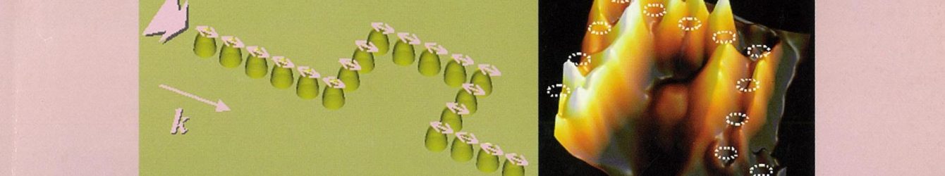
Nanodot couplers provide efficient near-field energy transfer Technical Report
2006, (SPIE Newsroom, November issue).
Links | BibTeX | タグ: Nanophotonic device, Nanophotonic fabrication
@techreport{SPIE,

title = {Nanodot couplers provide efficient near-field energy transfer},

author = {Takashi Yatsui and Wataru Nomura and Motoichi Ohtsu},

doi = {10.1117/2.1200610.0427},

year  = {2006},

date = {2006-11-02},

note = {SPIE Newsroom, November issue},

keywords = {Nanophotonic device, Nanophotonic fabrication},

pubstate = {published},

tppubtype = {techreport}

}
2005
八井崇、大津元一,
ナノ光デバイスとその製作―近接場光特有の動作と加工技術 Technical Report
2005, (O plus E,Vol. 27,No. 12、pp.1388-1392).
Links | BibTeX | タグ: Nanophotonic device, Nanophotonic fabrication
@techreport{opluse,

title = {ナノ光デバイスとその製作―近接場光特有の動作と加工技術},

author = {八井崇、大津元一},

url = {https://www.adcom-media.co.jp/bn/2005/11/25/17638/},

year  = {2005},

date = {2005-12-01},

urldate = {2005-12-01},

journal = {O plus E},

volume = {27},

pages = {1388-1392},

note = {O plus E,Vol. 27,No. 12、pp.1388-1392},

keywords = {Nanophotonic device, Nanophotonic fabrication},

pubstate = {published},

tppubtype = {techreport}

}
大津元一、八井崇、川添忠,
光の回折限界を超えるナノフォトニクスとその材料 Technical Report
2005, (工業材料7月号,Vol. 53,No. 7,pp.18-21).
BibTeX | タグ: Nanophotonic device, Nanophotonic material
@techreport{nanophotonicsb,

title = {光の回折限界を超えるナノフォトニクスとその材料},

author = {大津元一、八井崇、川添忠},

year  = {2005},

date = {2005-07-01},

urldate = {2005-07-01},

note = {工業材料7月号,Vol. 53,No. 7,pp.18-21},

keywords = {Nanophotonic device, Nanophotonic material},

pubstate = {published},

tppubtype = {techreport}

}
2004
八井崇、野村航、大津元一,
プラズモン・ポラリトンナノ光回路 Technical Report
2004, (光学,第33巻,第3号,pp.174-176).
Links | BibTeX | タグ: Nanophotonic device, Plasmon
@techreport{plasmon,

title = {プラズモン・ポラリトンナノ光回路},

author = {八井崇、野村航、大津元一},

url = {https://annex.jsap.or.jp/photonics/kogaku/public/33-03-gijutsu2.pdf},

year  = {2004},

date = {2004-03-01},

urldate = {2004-03-01},

note = {光学,第33巻,第3号,pp.174-176},

keywords = {Nanophotonic device, Plasmon},

pubstate = {published},

tppubtype = {techreport}

}